Technique method of metallization annealing of IGBT back face

A technology of backside metallization and process method, which is applied in the field of IGBT backside metallization and annealing, and can solve the problems of backside metal peeling and falling off.

Active Publication Date: 2015-10-21
SHANGHAI HUAHONG GRACE SEMICON MFG CORP
View PDF5 Cites 0 Cited by
  • Summary
  • Abstract
  • Description
  • Claims
  • Application Information

AI Technical Summary

Problems solved by technology

[0005] The technical problem to be solved by the present invention is to provide a process method for back metallization annealing of IGBT to solve the problem of back metal peeling off

Method used


Image

  • Technique method of metallization annealing of IGBT back face
  • Technique method of metallization annealing of IGBT back face
  • Technique method of metallization annealing of IGBT back face

Examples


Embodiment Construction

[0020] The metallization and annealing process on the back of the IGBT described in the present invention is applicable to all IGBT products of the non-TAIKO process, but not applicable to the wafers of the TAIKO process.

[0021] This process method comprises the following steps:

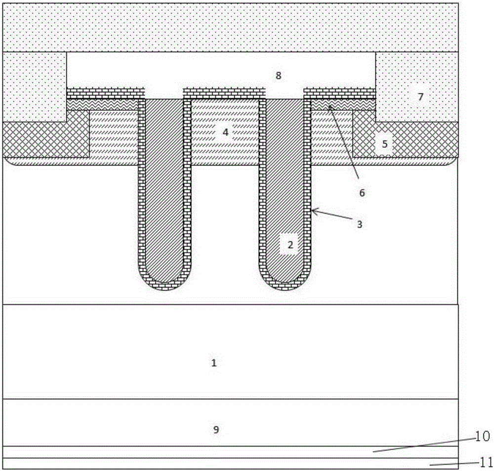
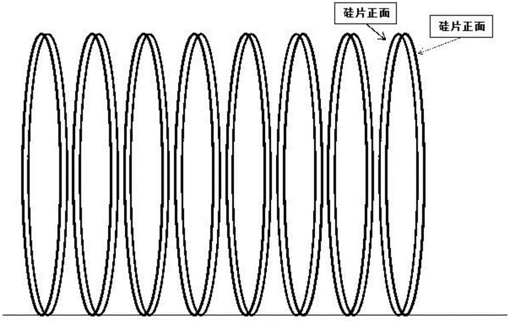
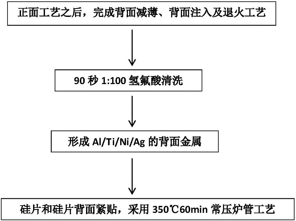
[0022] The first step is to select a suitable substrate to complete the front pattern process, including the cell area and the voltage protection ring area. After the front-side process is completed, thinning, back-side ion implantation, and back-side laser annealing processes are performed on the back side of the silicon wafer.

[0023] The second step is to clean the back of the silicon wafer with 1:100 buffered hydrofluoric acid for 90 seconds.

[0024] The third step is to deposit the back metal, that is to form the back metal of Al, Ti, Ni and Ag. Typical thicknesses correspond to 2000 angstroms, 2000 angstroms, 2000 angstroms, and 8000 angstroms, respectively.

[0025] In the fourth step, ...


PUM


Abstract

The invention discloses a technique method of metallization annealing of an IGBT back face. The technique method comprises steps of performing back face thinning, ion implantation and annealing technique after a front face technique is finished; performing 1:100 buffering hydrofluoric acid cleaning for 90 seconds; forming back face metal of Al, Ti, Ni and Ag; and tightly pasting a silicon sheet to a silicon sheet back face by using ordinary-pressure furnace tube technique of 350 DEG C for 60 minutes. According to the invention, while lower contact resistance of the back face metal of the silicon sheet is ensured, metal stripping is avoided, so an IGBT device is provided higher reliability.

Description

technical field [0001] The invention relates to the field of semiconductor device manufacturing, in particular to a process method for backside metallization annealing of an IGBT. Background technique [0002] IGBT (Insulated Gate Bipolar Transistor) Insulated Gate Bipolar Transistor is a composite fully-controlled voltage-driven power semiconductor device composed of BJT (Bipolar Transistor) and MOS (Insulated Gate Field Effect Transistor). The advantages of high input impedance and low conduction voltage drop of GTR. It has many excellent characteristics such as voltage control, large input impedance, low driving power, small on-resistance, and low switching loss. It is widely used in medium and high-power power electronic systems and is very suitable for transformers with DC voltages of 600V and above. Current systems, such as AC motors, frequency converters, switching power supplies, lighting circuits, traction drives and other fields. [0003] The IGBT is a backside l...

Claims


Application Information

Patent Timeline
Patent Type & Authority Applications(China)
IPC IPC(8): H01L29/40
CPCH01L29/401
Inventor 马彪
Owner SHANGHAI HUAHONG GRACE SEMICON MFG CORP
Why Eureka
Try Eureka