Manufacturing method of PCB integrated with multiple surface processing

A surface treatment and production method technology, which is applied in the secondary treatment of printed circuits, printed circuit manufacturing, cleaning/polishing of conductive patterns, etc., can solve the problems of single processing methods, avoid mutual interference, increase bonding force, and prevent being damaged The effect of plating on copper

Active Publication Date: 2015-10-21
JIANGMEN SUNTAK CIRCUIT TECH
View PDF3 Cites 22 Cited by
  • Summary
  • Abstract
  • Description
  • Claims
  • Application Information

AI Technical Summary

Problems solved by technology

[0004] The present invention aims at the problem that the existing PCB surface treatment method is single, and provides a PCB manufactur

Method used


Image

  • Manufacturing method of PCB integrated with multiple surface processing
  • Manufacturing method of PCB integrated with multiple surface processing

Examples


Embodiment

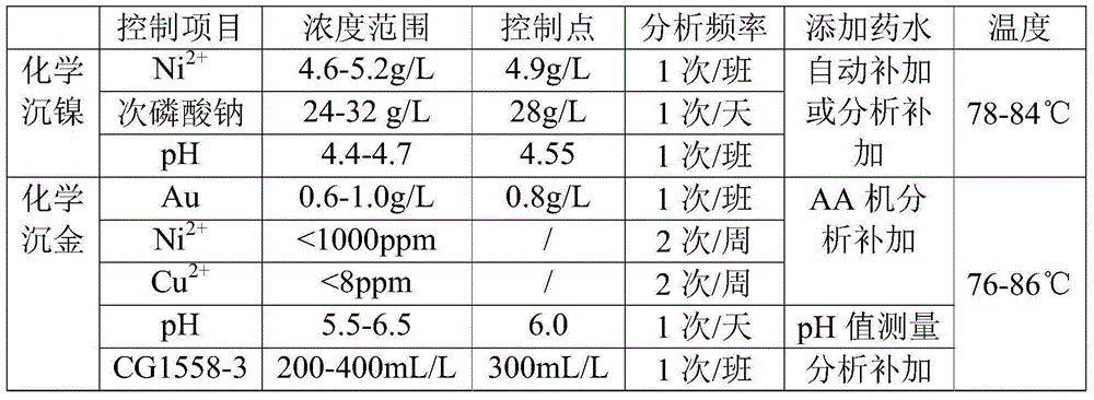
[0023] This embodiment provides a method for manufacturing a PCB with multiple surface treatments. The PCB is provided with an electric gold position, a nickel-immersion gold position, and an anti-oxidation position. The gold position is treated with immersion nickel gold surface treatment, and the anti-oxidation position is treated with anti-oxidation surface treatment.

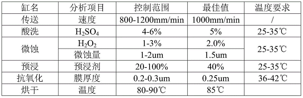
[0024] The specifications of the PCB are as follows: completed board thickness: 1.6mm; completed minimum aperture: 0.25mm; diameter-to-thickness ratio: 8:1; bottom copper thickness: 0.5OZ; local thick gold PAD (electrical gold position) gold thickness > 0.76um; Local immersion gold PAD (immersion nickel gold position) gold thickness > 0.05um; anti-oxidation film thickness (anti-oxidation position): 0.2-0.3um; minimum line width / spacing: 0.12 / 0.12mm.

[0025] The manufacturing method of the PCB comprises the following steps:

[0026] (1) Making multi-layer boards

[0027] According to the prior art, the cop...


PUM

PropertyMeasurementUnit
Thicknessaaaaaaaaaa
Thicknessaaaaaaaaaa
Thicknessaaaaaaaaaa

Abstract

The invention relates to the field of a PCB production and manufacturing technology, and specifically relates to a manufacturing method of a PCB integrated with multiple surface processing. Through adjusting the production process of the PCB, electroplating thick gold surface processing which is conventionally carried out only after a solder mask is manufactured is performed in advance before an external-layer line is prepared, corresponding technical parameters are adjusted, the problem of mutual interference of three surface processing is effectively avoided, and three surface processing modes are realized in the same PCB. According to the invention, through adjusting a process sequence and the technical parameters, when antioxidation surface processing is carried out, the gold layer at an electroplating gold position and a nickel gold immersion position is not oxidized and an organic membrane is not formed, such that the effects of various surface processing are ensured. When the external-layer line is prepared, a volcanic ash grinding plate is employed, the bonding force applied to a dry membrane and a plate surface in a positive process can be increased, and the electroplating gold position is prevented from being plated with copper during pattern electroplating.

Description

technical field [0001] The invention relates to the technical field of PCB production and manufacturing, in particular to a method for manufacturing a PCB with various surface treatments. Background technique [0002] Surface treatment is the last process in the manufacturing process of PCB (Printed Circuit Board, printed circuit board). Surface treatment is to coat a layer of protective material on the copper surface of PCB to protect the copper surface of PCB and facilitate the welding of circuit board pads. properties and corrosion resistance. Common surface treatment methods include Immersion Gold, Immersion Silver, Immersion Tin, Electroplated Nickel Gold (Flash Gold), Leaded HASL, Lead-free HASL -LF), antioxidant (OSP) and light copper (Naked Copper). [0003] With the rapid development of electronic technology and the harsh use environment, a single surface treatment on PCB cannot meet customer requirements, and it is becoming more and more urgent to develop a combi...

Claims


Application Information

Patent Timeline
IPC IPC(8): H05K3/22H05K3/26H05K3/28
CPCH05K3/22H05K3/241H05K3/28
Inventor 陈勇武李渊张义兵华荣双
Owner JIANGMEN SUNTAK CIRCUIT TECH
Why Eureka
Try Eureka