Scanning electron microscope probe current detection device and scanning electron microscope

A technology of a current detection device and a scanning electron microscope, applied in the field of electron optics, can solve the problems of extremely high precision requirements of the sample stage and low current efficiency of the detection probe, and achieve the effect of reducing the precision requirements

Active Publication Date: 2015-10-28
KYKY TECH
View PDF4 Cites 1 Cited by
  • Summary
  • Abstract
  • Description
  • Claims
  • Application Information

AI Technical Summary

Problems solved by technology

[0007] For this reason, the technical problem to be solved by the present invention is that the detection probe current efficiency in the scanning electron microscope in the prior art is low, and the precision of the sample stage is extremely high.

Method used


Image

  • Scanning electron microscope probe current detection device and scanning electron microscope
  • Scanning electron microscope probe current detection device and scanning electron microscope
  • Scanning electron microscope probe current detection device and scanning electron microscope

Examples


Embodiment 1

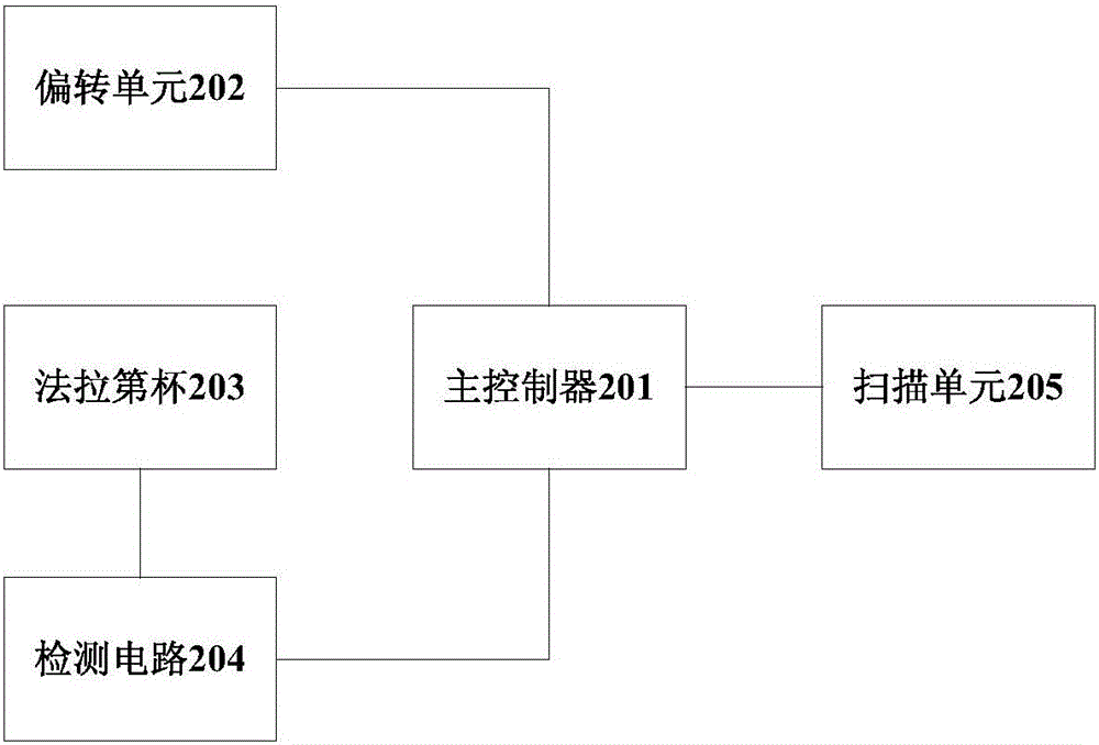
[0040] This embodiment provides a scanning electron microscope probe current detection device, which is arranged in the lens barrel of the scanning electron microscope, such as figure 2 As shown, it includes a main controller 201, a deflection unit 202, a Faraday cup 203 and a detection circuit 204, wherein:

[0041] The deflection unit 202 is arranged between the electron beam generator and the scanning unit, receives the electron beam emitted by the electron beam generator, and controls whether the electron beam is deflected.

[0042] The Faraday cup 203 is arranged in the deflection direction of the electron beam output by the deflection unit, and collects the deflected electron beam.

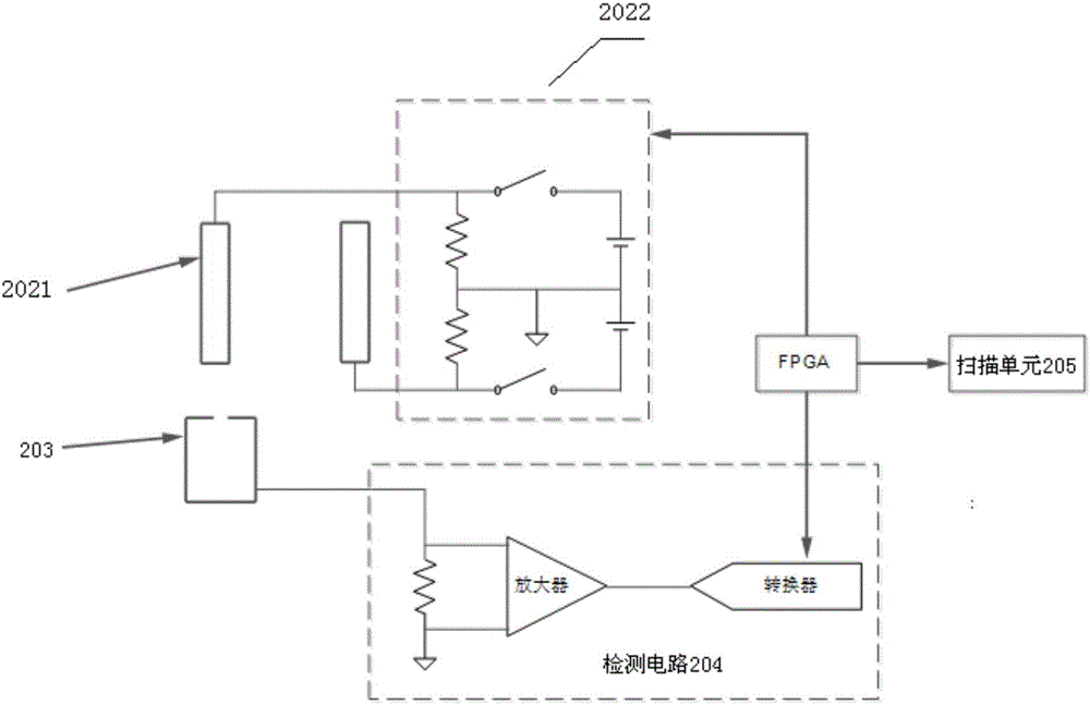
[0043] The detection circuit 204 is configured to detect the electron beam collected in the Faraday cup 203 .

[0044] The main controller 201 is used to control the working state of the deflection unit 202, the Faraday cup 203 and the scanning unit 205, so as to realize:

[0045] When th...

Embodiment 2

[0050] This embodiment provides a scanning electron microscope, including the scanning electron microscope probe current detection device provided in Embodiment 1, an electron beam generator and a scanning unit. Wherein the electron beam generator is used to generate and emit electron beams, and the scanning unit is used to control the deflection of the electron beams entering it, and perform two-dimensional scanning on the samples on the sample stage. Specifically, such as Figure 4 As shown, the electron beam generator includes an electron gun 401 , a condenser lens 402 and a movable diaphragm 403 . The electron gun 401 generates electron beams, and the condenser lens 402 converges the electron beams generated by the electron gun 401 and transmits them to the movable diaphragm 403 , and the movable diaphragm 403 limits the aperture angle of the electron beams. The scanning unit includes an objective lens 408 and a deflection coil 409. The objective lens 408 converges the el...


PUM


Abstract

The present invention provides a scanning electron microscope probe current detection device and a scanning electron microscope. When a scanning unit is in a forward scan stage, a deflection unit controls an electron beam not to deflect, a detection circuit does not carry out the sampling operation of the electron beam, at this time, the electron beam passes a lens cone normally to irradiate to the surface of a sample, thereby realizing the sample imaging. When the scanning unit is in a flyback stage, the deflection unit controls the electron beam to deflect, the detection circuit carries out the sampling operation of the electron beam, so that a numerical value of a probe current is obtained. The whole process does not need to move a sample bench completely. The electron beam does not participate in the imaging in the flyback stage, so that the image acquisition of the scanning electron microscope is not interrupted when the probe current is detected in the flyback stage, the change of the probe current is detected real-timely while the electron microscope images are acquired, and the probe current detection is finished efficiently. Meanwhile, the probe current detection does not need to move the sample bench, so that the precision requirement of the sample bench can be reduced.

Description

technical field [0001] The invention relates to the technical field of electron optics, in particular to a scanning electron microscope probe current detection device and a scanning electron microscope. Background technique [0002] Scanning electron microscope, referred to as scanning electron microscope, is an electronic optical instrument that uses focused electron beams to scan the surface of the sample line by line. The efficiency of electron beam bombardment of the sample surface to generate secondary electrons or backscattered electrons is related to the surface morphology or material of the sample. . Collect the secondary electrons or backscattered electrons generated on the surface of the sample, and represent the scanning position of the electron beam on the surface of the sample and the number of secondary electrons or backscattered electrons generated in the form of a two-dimensional image, that is, obtain the secondary electron image of the scanning electron mic...

Claims


Application Information

Patent Timeline
Patent Type & Authority Applications(China)
IPC IPC(8): H01J37/28H01J37/244G01R19/00
Inventor 王大千孟祥良
Owner KYKY TECH
Why Eureka
Try Eureka