Silicon controlled rectifier

A technology of silicon-controlled rectifier and doped region, which is applied to electric solid-state devices, semiconductor devices, semiconductor/solid-state device components, etc., can solve the problems of increasing the size of silicon-controlled rectifiers, increasing the complexity and cost of overall circuit design, etc. Achieve the effect of increasing the holding voltage and expanding the application range

Inactive Publication Date: 2015-11-04
RICHTEK TECH
10 Cites 0 Cited by

AI-Extracted Technical Summary

Problems solved by technology

However, increasing the channel length of the silicon-controlled rectifier will inevitably lead to an increase in the size of the silicon-controlled rectifier, and the use...

Method used

[0026] In order to increase the holding voltage of the silicon controlled rectifier 100, the ion doping concentration of the first P-type doped region 124 can be designed to be lower than eight percent of the ion doping concentration of the second P-type doped region 134 ten. In one embodiment, the ion doping concentration of the first P-type doped region 124 can be designed to be lower than two-thirds of the ion doping conce...

Abstract

The invention provides a silicon controlled rectifier comprising a substrate; an N well region and a P well region which are arranged at the first side of the substrate and adjacent to each other; a first N-type doped region and a first P-type doped region which are arranged at the upper surface of the N well region and adjacent to each other; a second N-type doped region and a second P-type doped region which are arranged at the upper surface of the P well region; a first oxidation isolation region which isolates the first P-type doped region and the second N-type doped region; a second oxidation isolation region which isolates the second N-type doped region and the second P-type doped region; an anode end which is coupled with the first N-type doped region and the first P-type doped region; and a cathode end which is coupled with the second N-type doped region and the second P-type doped region. Ion doping concentration of the first P-type doped region is lower than that of the second P-type doped region for eighty percent. According to the framework of the silicon controlled rectifier, sustaining voltage of the silicon controlled rectifier can be effectively enhanced without increasing channel length or using additional auxiliary circuit.

Application Domain

Semiconductor/solid-state device detailsSolid-state devices +1

Technology Topic

P type dopingIon doping +5

Image

  • Silicon controlled rectifier

Examples

  • Experimental program(1)

Example Embodiment

[0022] The embodiments of the present invention will be described below in conjunction with related drawings. In the drawings, the same reference numerals indicate the same or similar elements or method flows.
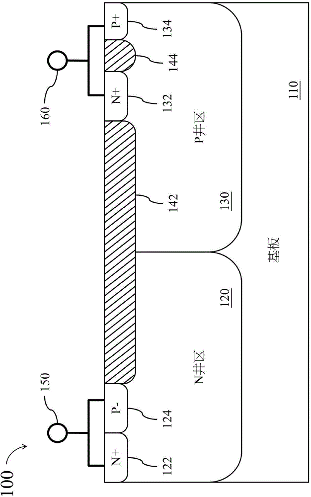
[0023] figure 1 This is a simplified cross-sectional view of the silicon controlled rectifier 100 according to an embodiment of the present invention. The silicon controlled rectifier 100 includes a substrate 110, an N well region (N well) 120, a P well region (P well) 130, a first N-type doped region (N region) 122, a A first P-type doped region (P region) 124, a second N-type doped region 132, a second P-type doped region 134, and a first oxide isolation region 142. A second oxide isolation region 144, an anode terminal 150, and a cathode terminal 160.
[0024] Such as figure 1 As shown, the N-well region 120 is disposed on a first side of the substrate 110. The P-well area 130 is disposed on the first side of the substrate 110 and is adjacent to the N-well area 120. The first N-type doped region 122 is disposed on an upper surface of the N-well region 120. The first P-type doped region 124 is disposed on the upper surface of the N-well region 120 and is adjacent to the first N-type doped region 122. The second N-type doped region 132 and the second P-type doped region 134 are both disposed on an upper surface of the P-well region 130. The first oxide isolation region 142 is disposed in a partial area of ​​the upper surface of the N-well region 120 and a partial area of ​​the upper surface of the P-well region 130, and isolates the first P-type doped region 124 and the second N-type doped region 132. The second oxide isolation region 144 is disposed in a partial area of ​​the upper surface of the P-well region 130 and isolates the second N-type doped region 132 and the second P-type doped region 134. The anode terminal 150 is coupled to the first N-type doped region 122 and the first P-type doped region 124. The cathode terminal 160 is coupled to the second N-type doped region 132 and the second P-type doped region 134.
[0025] In practice, both the N-well region 120 and the P-well region 130 can be directly located on the first side of the substrate 110. Alternatively, the N-well region 120 and the P-well region 130 may both be disposed above the first side of the substrate 110, and there is another layer structure between the substrate 110, such as an isolation layer. In addition, the aforementioned first N-type doped region 122 and second N-type doped region 132 are both an N+ doped region (heavily doped N region), and the second P-type doped region The region 134 is a P+ doped region (heavily doped P region). The substrate 110 can be implemented by an N-type buried layer or a P-type buried layer.
[0026] In order to increase the holding voltage of the silicon controlled rectifier 100, the ion doping concentration of the first P-type doping region 124 can be designed to be lower than 80% of the ion doping concentration of the second P-type doping region 134. In an embodiment, the ion doping concentration of the first P-type doped region 124 may be designed to be lower than two-thirds of the ion doping concentration of the second P-type doped region 134 to further improve the silicon-controlled rectifier 100 holding voltage.
[0027] In another embodiment, the ion doping concentration of the first P-type doping region 124 can be designed to be lower than one third of the ion doping concentration of the second P-type doping region 134 to further increase The holding voltage of the silicon controlled rectifier 100.
[0028] For example, the ion doping concentration of the first P-type doped region 124 can be designed to be in the range of 1E13 ions per cubic centimeter to 1E14 ions per cubic centimeter, and the ions of the second P-type doped region 134 can be doped The impurity concentration is designed to be greater than 3E14 ions per cubic centimeter.
[0029] In practice, the aforementioned first P-type doped region 124 can be implemented by a P-doped region (lightly doped P region).
[0030] In the foregoing embodiment, since the ion doping concentration of the first P-type doped region 124 in the silicon controlled rectifier 100 is lower than eighty or three percent of the ion doping concentration of the second P-type doped region 134 The second, or even one-third, can reduce the number of holes in the channel of the silicon controlled rectifier 100, thereby effectively increasing the channel length of the silicon controlled rectifier 100 and the use of additional auxiliary circuits. The holding voltage of the silicon controlled rectifier 100.
[0031] In this way, the holding voltage of the silicon controlled rectifier 100 can exceed the operating voltage of many high-voltage integrated circuits, so that the silicon controlled rectifier 100 can be used as an electrostatic protection device for high-voltage integrated circuits with an operating voltage above 10V. For example, the anode terminal 150 of the silicon controlled rectifier 100 can be coupled to the power pin of a high-voltage integrated circuit with an operating voltage above 10V, and the cathode terminal 160 can be coupled to a ground terminal to utilize the silicon controlled rectifier 100 is used as an electrostatic protection device for the power supply pin.
[0032] In other words, the structure of the aforementioned silicon-controlled rectifier 100 can greatly expand the application range of the silicon-controlled rectifier 100, so that the silicon-controlled rectifier 100 can be more widely used for electrostatic protection of various high-voltage integrated circuits.
[0033] Certain words are used in the description and claims to refer to specific elements. However, those skilled in the art should understand that the same element may be called by different terms. The specification and claims do not use differences in names as a way to distinguish elements, but use differences in functions of elements as a basis for distinction. The "including" mentioned in the specification and claims is an open term, so it should be interpreted as "including but not limited to." In addition, "coupling" here includes any direct and indirect connection means. Therefore, if the text describes that the first element is coupled to the second element, it means that the first element can be directly connected to the second element through electrical connection, wireless transmission, optical transmission, or other signal connection methods, or through other elements or connections. The means is indirectly connected to the second element electrically or signally.
[0034] The description method of "and/or" used herein includes any combination of one or more of the listed items. In addition, unless otherwise specified in the specification, any term in the singular case also includes the meaning of the plural case.
[0035] The term "element" mentioned in the specification and claims includes the concept of component, layer, or region.
[0036] The size and relative size of some elements in the drawings will be enlarged, or the shape of some elements will be simplified, so as to more clearly express the content of the embodiments. Therefore, unless otherwise specified by the applicant, the shape, size, relative size, and relative position of each element in the drawings are only for convenience of description, and should not be used to limit the scope of the patent of the present invention. In addition, the present invention can be embodied in many different forms, and when explaining the present invention, it should not be limited to the embodiments presented in this specification.
[0037] For the convenience of description, some descriptions related to relative positions in space may be used in the description to describe the function of an element in the drawings or the relative spatial relationship between the element and other elements. For example, "above...", "above...", "below", "below...", "above...", "below...", "up", "down", etc. Those skilled in the art should understand that these descriptions related to relative positions in space not only include the orientation of the described elements in the drawings, but also include the use, operation, or operation of the described elements. Various pointing relationships during assembly. For example, if the figure is turned upside down, the elements originally described as "on" will become "below". Therefore, in the description of the description of "于...上" used in the manual, the explanation includes two different directional relationships: "于...下" and "于...上". In the same way, the term "up" used here is interpreted as including two different directional relationships, "up" and "down".
[0038] In the specification and claims, if it is described that the first element is located on, above the second element, connected, joined, coupled to, or connected to the second element, it means that the first element can be directly connected to the second element. Being located on the second element, directly connected, directly bonded, or directly coupled to the second element can also indicate that there are other elements between the first element and the second element. In contrast, if it is described that the first element is directly located on, directly connected, directly joined, directly coupled, or directly connected to the second element, it means that there are no other elements between the first element and the second element. .
[0039] The above are only preferred embodiments of the present invention, and all equivalent changes and modifications made in accordance with the claims of the present invention should fall within the scope of the present invention.

PUM

no PUM

Description & Claims & Application Information

We can also present the details of the Description, Claims and Application information to help users get a comprehensive understanding of the technical details of the patent, such as background art, summary of invention, brief description of drawings, description of embodiments, and other original content. On the other hand, users can also determine the specific scope of protection of the technology through the list of claims; as well as understand the changes in the life cycle of the technology with the presentation of the patent timeline. Login to view more.

Similar technology patents

Novel ESD protection structure and realizing method thereof

ActiveCN107248514AIncrease holding voltage
Owner:SHANGHAI HUALI MICROELECTRONICS CORP

Carbon dioxide-slickwater intermittent mixed-fracturing design method

InactiveCN108729897AImprove fracturing effectExpand the scope of application
Owner:CHINA UNIV OF PETROLEUM (BEIJING)

Classification and recommendation of technical efficacy words

  • Expand the scope of application
  • Increase holding voltage

Distributed optical fiber vibration sensing method and apparatus thereof

ActiveCN1862239AAvoid restrictions on use occasions and environmentsExpand the scope of application
Owner:武汉光谷光联网科技有限公司

Method for converting flash animation data into hypertext markup language (HTML) 5 data

ActiveCN103176986AImprove conversion speedExpand the scope of application
Owner:SHANGHAI PATEO ELECTRONIC EQUIPMENT MANUFACTURING CO LTD

Novel ESD protection structure and realizing method thereof

ActiveCN107248514AIncrease holding voltage
Owner:SHANGHAI HUALI MICROELECTRONICS CORP
Why Eureka
Try Eureka