Thin-film transistor, manufacturing method thereof, array substrate and display device

A technology of thin film transistor and manufacturing method, which is applied in the direction of transistor, semiconductor/solid-state device manufacturing, electric solid-state device, etc., can solve the problems of large equipment loss, difficult mass production, and low yield rate.

Inactive Publication Date: 2015-11-11
BOE TECH GRP CO LTD +1
View PDF4 Cites 13 Cited by
  • Summary
  • Abstract
  • Description
  • Claims
  • Application Information

AI Technical Summary

Problems solved by technology

[0004] In the above-mentioned steps of the existing TFT array substrate manufacturing process, the source-drain metal layer thin film has undergone a wet etching and a dry etching, wherein in the dry etching process, for the source corresponding to the channel region There are various disadvantages when etching the drain metal layer. For example, it is difficult to etch the metal layer by dry etching equipment, and the etching is uneven, the equipment loss is large, and the yield is low. It is difficult to apply to mass production.

Method used


Image

  • Thin-film transistor, manufacturing method thereof, array substrate and display device
  • Thin-film transistor, manufacturing method thereof, array substrate and display device
  • Thin-film transistor, manufacturing method thereof, array substrate and display device

Examples


Embodiment Construction

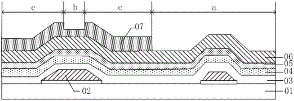
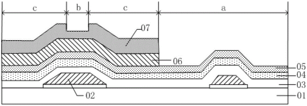
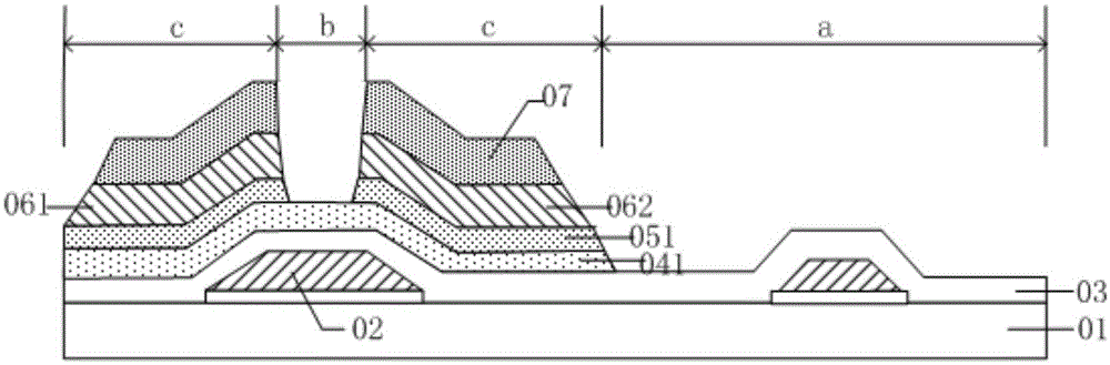
[0039] The specific implementation manners of the thin film transistor, the manufacturing method thereof, the array substrate and the display device provided by the embodiments of the present invention will be described in detail below with reference to the accompanying drawings.

[0040] Wherein, the thickness and shape of each film layer in the drawings do not reflect the real scale of the thin film transistor, and the purpose is only to illustrate the content of the present invention.

[0041] An embodiment of the present invention provides a method for manufacturing a thin film transistor, such as figure 2 shown, including:

[0042] S201, sequentially forming a gate pattern, a gate insulating layer film, an active layer film and an ohmic contact layer film on the base substrate;

[0043] S202, forming a first etch stop module on the ohmic contact layer film in the channel region to be formed;

[0044] S203, forming a source-drain metal layer thin film on the base substr...


PUM


Abstract

The invention discloses a thin-film transistor, a manufacturing method thereof, an array substrate and a display device. The method includes the steps that a grid graph, a gate insulation layer thin film, an active layer thin film, an ohmic contact layer thin film, a first etching blocking module and a source drain metal layer thin film are sequentially formed on a substrate base plate, wherein the first etching blocking module and the source drain metal layer thin film are located in a channel region to be formed; the first etching blocking module shields the active layer thin film and the ohmic contact layer thin film corresponding to the channel region to be formed, and the graph containing source and drain is formed through wet etching; the graph containing an ohmic contact layer and an active layer is formed through a dry etching technology. According to the thin-film transistor, the manufacturing method thereof, the array substrate and the display device, on the basis that the first etching blocking module can protect the active layer thin film corresponding to the channel region to be formed, etching of the source metal layer and the drain metal layer is completed just through a wet etching technology, etching is even, and the problems that when the dry etching technology is adopted to etch the source metal layer and the drain metal layer, etching is uneven, the equipment loss is large, and the yield is low are solved.

Description

technical field [0001] The invention relates to the field of display technology, in particular to a thin film transistor, a manufacturing method thereof, an array substrate and a display device. Background technique [0002] Generally, a thin-film transistor (Thin-film Transistor, TFT) plays a very important role in an array substrate. [0003] At present, in the manufacturing process of thin film transistors, it specifically includes: step 1, such as Figure 1a As shown, the pattern of the gate 02, the gate insulating layer film 03, the active layer film 04, the ohmic contact layer film 05, the source-drain metal layer film 06, and the photoresist layer film 07 are sequentially formed on the base substrate 01, The photoresist layer film 07 is exposed and developed to obtain the photoresist completely removed region a, the photoresist partially retained region b and the photoresist completely retained region c, the photoresist completely removed region a corresponds to the a...

Claims


Application Information

Patent Timeline
Patent Type & Authority Applications(China)
IPC IPC(8): H01L29/786H01L21/336H01L27/12
CPCH01L27/1214H01L29/66742H01L29/786H01L27/1288H01L29/66765H01L29/66969H01L29/78618H01L29/78669H01L29/78678H01L21/0274H01L21/30604H01L21/3081H01L21/32135H01L21/32139
Inventor 熊胜楠郑云友李伟张益存
Owner BOE TECH GRP CO LTD
Why Eureka
Try Eureka