A near field communication antenna device

A near-field communication antenna and antenna device technology, which is applied in the direction of antenna support/installation device, antenna, loop antenna, etc., can solve the problems of destroying the integrity of the conductor layer, effect impact, attenuation, etc., and achieve convenient appearance design and improved design effect of space

Active Publication Date: 2018-01-12
UNIV OF ELECTRONICS SCI & TECH OF CHINA
View PDF6 Cites 0 Cited by
  • Summary
  • Abstract
  • Description
  • Claims
  • Application Information

AI Technical Summary

Problems solved by technology

[0004] However, the solution provided by it has the following problems: 1. The structure of this scheme needs to open a hole in the conductor layer covered by the antenna, and needs to make a gap on one side of the hole, which structurally destroys the integrity of the conductor layer. The design of the shell structure of the equipment does not allow openings to damage its appearance integrity or structural support characteristics, so this solution is subject to great application restrictions; 2. In this solution, the electromagnetic field generated by the antenna needs to bypass the conductor layer, and the electromagnetic field In the process of bypassing the conductor layer, the conductor layer will cause greater attenuation to the electromagnetic field, and the degree of attenuation is related to the length of the conductor layer bypassed. The solution is that the antenna is assembled on a wider conductor layer, that is, when the metal casing moves larger In the device terminal, its effect will be affected

Method used


Image

  • A near field communication antenna device
  • A near field communication antenna device
  • A near field communication antenna device

Examples


Embodiment approach 1

[0036] Make a 40mm×40mm area, ordinary 0.8mm line width single-layer conductor antenna with 4 turns design, the bottom is equipped with magnetic materials, and the surface of the coil conductor is not covered by a conductor layer, which is recorded as an ordinary antenna device; the area of ​​the antenna device is 40mm×40mm, and the area The wire width of the 4-part coil conductor is 1.2 mm, the wire width of the coil conductor in the area 3 is 0.3 mm, the overall design is 5 turns, the bottom is equipped with magnetic materials, and the surface of the coil conductor of the antenna device is covered with a conductor layer, so that the width of the area 3 part is 4 mm, which is recorded as the present invention Design the antenna device; the area of ​​the antenna device is 40mm×40mm, and the common line width is 0.8mm. The single-layer antenna has 4 turns, the bottom is equipped with magnetic materials, and the conductor layer is also covered on the antenna device, and the leakag...

Embodiment approach 2

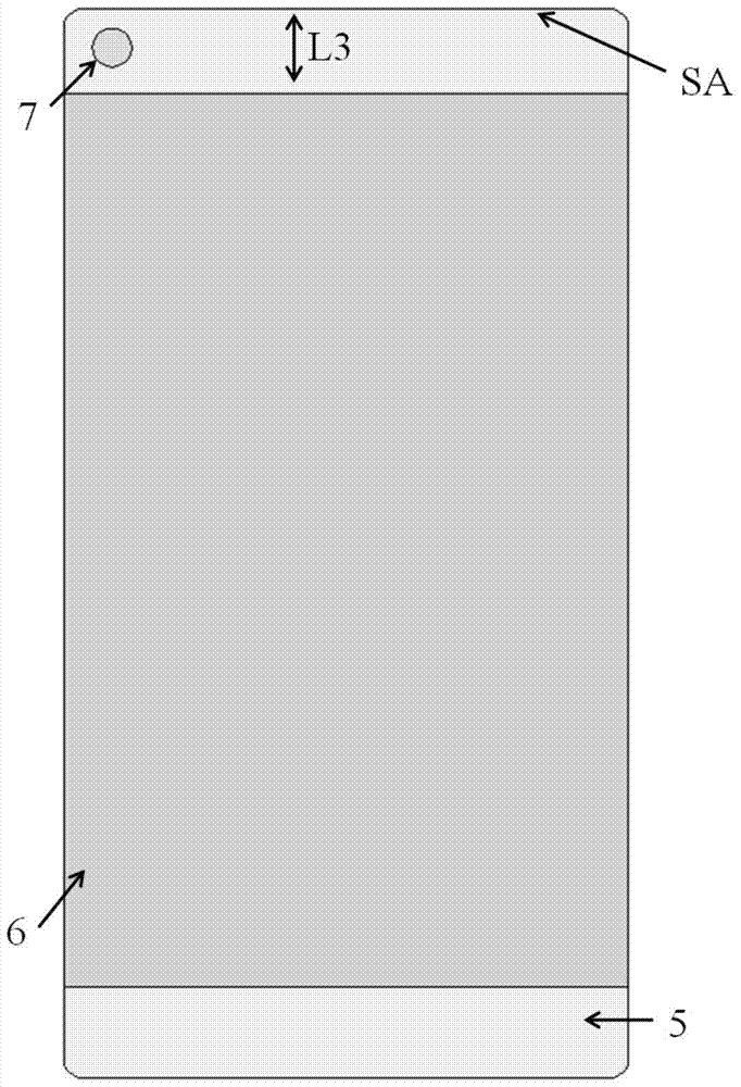
[0040] Electronic equipment enclosures remain figure 1 structure in the rear of the electronic device. figure 1 The middle L3 is longer, which can leave a wider space for the three parts of the antenna device of the present patent invention, and the coil conductor 1 in the area 3 is designed with unequal line widths to achieve better communication effects.

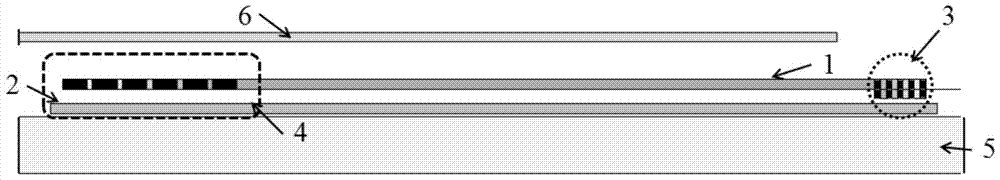
[0041] If the length of L3 is longer, the interlayer structure of the realized antenna device is as follows: image 3 As described in the antenna device, the specific details of the antenna device are as follows Figure 4 In the antenna setup shown, Figure 4 In the middle area 3 part, the width of this part is 6 mm, and its coil conductors are designed in steps with unequal widths, and the line width of the coil conductor 1 in area 3 is designed in an equal difference from the outside to the inside. Finally realized as Figure 4 The structure of the antenna device.

[0042] Such as Figure 4 The structure in the ant...

Embodiment approach 3

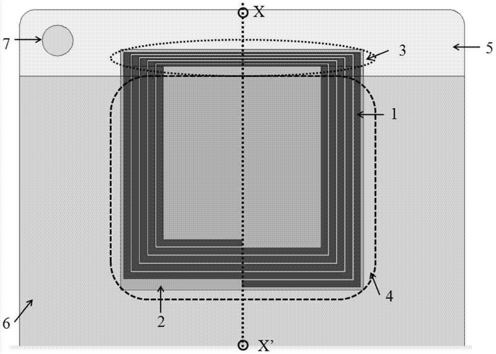
[0044] The rear structure of the electronic equipment housing is as follows: Figure 5 shown, compared figure 2 The rear structure of the electronic equipment in , the difference is that the opening design is carried out in the shell conductor layer 6, and the position of the opening 7 is selected to surround the spare part in the center of the coil conductor 1 in the antenna device, but the opening Edges do not form break gaps.

[0045] In the 6 parts of the outer casing conductor layer, the center of the coil conductor in the antenna device is opened around the spare part. After the hole is opened, a larger electromagnetic wave entry window is provided for the antenna device, which can further improve the communication distance of the antenna device.

[0046] The interlayer structure of the antenna device is as follows image 3 The antenna assembly described in.


PUM


Abstract

The invention belongs to the field of wireless communication, and relates to an antenna device used in a short-distance wireless communication system. The antenna device is an antenna device formed in a mobile electronic device, including: a coil conductor, a flexible substrate, a magnetic material and a shell conductor layer. The coil conductor is an annular or helical coil with the winding center as the coil opening, and the flexible substrate attached to it is assembled on the surface of the magnetic sheet material. The shell conductor layer divides the shielding of the coil conductor into two areas: the first area is the shielding part of the non-shell conductor layer, that is, the actual magnetic link coupling part of the antenna, and the coil conductor of this part adopts a narrow line width design or most of it adopts a narrow line width design , and use the parallel design of double conductor layers; the second area is the shielding part of the shell conductor layer, and the coil conductor in this area is designed with wide lines. The invention has the positive effects of not destroying the structural integrity of the metal part of the casing of the mobile device, occupying a small space and having high performance.

Description

technical field [0001] The present invention relates to an antenna device used in an RFID system, an NFC system, and a short-distance wireless communication system that communicate with a counterpart device through an electromagnetic field signal. Background technique [0002] In recent years, with the continuous promotion and use of RFID systems and NFC systems, especially the promotion and application of NFC systems in the financial field. In order to communicate between mobile electronic devices or between mobile electronic devices and basic card reading devices, each device, especially the handheld mobile electronic device, is equipped with a communication antenna for the NFC system. Due to the line width, the existing RFID or NFC antennas are mostly designed with 3 to 4 turns, and are assembled inside the casing of the mobile device. With the emergence of mobile electronic devices equipped with metal casings, the service life of mobile electronic devices and the wear r...

Claims


Application Information

Patent Timeline
Patent Type & Authority Patents(China)
IPC IPC(8): H01Q1/22H01Q7/00H01Q1/42
Inventor 邓龙江李维佳梁迪飞谢建良阙志勇周毅然
Owner UNIV OF ELECTRONICS SCI & TECH OF CHINA
Why Eureka
Try Eureka