Low-power-consumption phase change film material for multistage phase change storage, and reparation method and application thereof

A technology of phase change storage and thin film materials, applied in electrical components and other directions, can solve the problems of slow phase change speed and high power consumption, and achieve the effect of improving storage density, reducing power consumption and increasing storage density.

Inactive Publication Date: 2015-11-18
TONGJI UNIV
View PDF4 Cites 9 Cited by
  • Summary
  • Abstract
  • Description
  • Claims
  • Application Information

AI Technical Summary

Problems solved by technology

However, the thin film material involved in this invention has a larger threshold (8.5V) and SET (4.0V, 1000ns) voltage, indicating that the thin film has larger power consumption and slower phase transition speed than traditional GST materials, to be further improved

Method used


Image

  • Low-power-consumption phase change film material for multistage phase change storage, and reparation method and application thereof
  • Low-power-consumption phase change film material for multistage phase change storage, and reparation method and application thereof
  • Low-power-consumption phase change film material for multistage phase change storage, and reparation method and application thereof

Examples


Embodiment 1

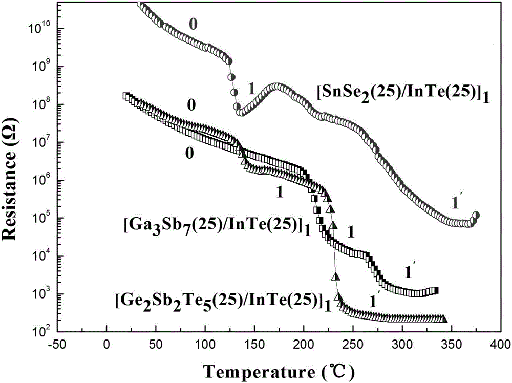
[0029] The single-layer InTe phase-change film prepared in this example has a total thickness of 50 nm.

[0030] 1. Clean SiO2 2 / Si(100) substrate:

[0031] (a) Place the substrate in deionized water, and clean it ultrasonically for 20 minutes to remove dust particles on the surface of the substrate;

[0032] (b) Place the substrate in absolute ethanol, and clean it ultrasonically for 20 minutes to remove dust particles and inorganic impurities on the surface of the substrate;

[0033] (c) repeating step (b) three times;

[0034] (d) Take out the substrate, dry it with pure Ar gas, and set it aside.

[0035] 2. Preliminary preparation for sputtering InTe film:

[0036] (a) Place the InTe target on the No. 1 target position, fix the processed substrate on the sample stage, and close the sealed vacuum chamber;

[0037] (b) Turn on the mechanical pump and preheat the molecular pump for 5 minutes. When the vacuum reaches 5Pa or below, start the molecular pump and pump the va...

Embodiment 2

[0042] This example prepares InTe-Ga 3 Sb 7 Nanocomposite film, the composition is [InTe(25nm) / Ga 3 Sb 7 (25nm)] 1 , with a total thickness of 50 nm.

[0043] 1. Clean SiO2 2 / Si(100) substrate:

[0044] (a) Place the substrate in deionized water, and clean it ultrasonically for 20 minutes to remove dust particles on the surface of the substrate;

[0045] (b) Place the substrate in absolute ethanol, and clean it ultrasonically for 20 minutes to remove dust particles and inorganic impurities on the surface of the substrate;

[0046] (c) repeating step (b) three times;

[0047] (d) Take out the substrate, dry it with pure Ar gas, and set it aside.

[0048] 2. Sputtering [InTe(25nm)-Ga 3 Sb 7 (25nm)] 1 Film preparation:

[0049] (a) Combine InTe and Ga 3 Sb 7 The targets are respectively placed on the No. 1 and No. 2 target positions, and the processed substrate is fixed on the sample stage, and the sealed vacuum chamber is closed;

[0050] (b) Turn on the mechanic...

Embodiment 3

[0057] Preparation of InTe-Ge 2 Sb 2 Te 5 Nanocomposite film, the composition is [InTe(25nm) / Ge 2 Sb 2 Te 5 (25nm)] 1 , with a total thickness of 50 nm.

[0058] 1. Clean SiO2 2 / Si(100) substrate:

[0059] (a) Place the substrate in deionized water, and clean it ultrasonically for 20 minutes to remove dust particles on the surface of the substrate;

[0060] (b) Place the substrate in absolute ethanol, and clean it ultrasonically for 20 minutes to remove dust particles and inorganic impurities on the surface of the substrate;

[0061] (c) repeating step (b) three times;

[0062] (d) Take out the substrate, dry it with pure Ar gas, and set it aside.

[0063] 2. Sputtering [InTe(25nm)-Ge 2 Sb 2 Te 5 (25nm)] 1 Film preparation:

[0064] (a) Combine InTe and Ge 2 Sb 2 Te 5 The targets are respectively placed on the No. 1 and No. 2 target positions, and the processed substrate is fixed on the sample stage, and the sealed vacuum chamber is closed;

[0065] (b) Tur...


PUM

PropertyMeasurementUnit
thicknessaaaaaaaaaa
thicknessaaaaaaaaaa
thicknessaaaaaaaaaa

Abstract

The invention relates to a low-power-consumption phase change film material for multistage phase change storage, and a preparation method and an application thereof. A chemical component of the thin material is InTe([alpha])-X([alpha]), wherein [alpha] is the thickness of a single-layer InTe film and the thickness of a single-layer X film; and, on a SiO<2> / Si (100) substrate, InTe and Ga<3>Sb<7>, SnSe<2> or Ge<2>Sb<2>Te<5> are taken as target materials, argon is taken as a glow gas, an InTe film and a Ga<3>Sb<7>, SnSe<2> or Ge<2>Sb<2>Te<5> film are alternatively deposited, and then the low-power-consumption phase change film material for the multistage phase change storage is obtained through preparation. Compared with the prior art, the low-power-consumption phase change film contains a relative traditional semiconductor material Te in a phase change storage field, also contains an element In which can increase and stabilize a value of an amorphous resistor, and forms a large high-low resistor.

Description

technical field [0001] The invention relates to materials in the field of microelectronic technology, in particular to a low-power phase-change thin-film material for multi-level phase-change storage and its preparation method and application. Background technique [0002] Memory, as the core component of electronic equipment, is playing an increasingly important role in the 21st century of information globalization. Phase Change Random Access Memory (PCRAM) is a non-volatile memory, which has the advantages of small storage unit size, long cycle life, good stability, low power consumption and strong embedded function, and has become the most promising alternative to the memory widely used in the market today. (FLASH). In addition, the PCRAM manufacturing process is compatible with the CMOS process and has low cost, which also indicates the prospect of its wide application (J. Hegedüsand S.R. Elliott: Nature, 2008, p.399). [0003] Ge-Sb-Te system alloy phase change materi...

Claims


Application Information

Patent Timeline
Patent Type & Authority Applications(China)
IPC IPC(8): H01L45/00
Inventor 翟继卫刘瑞蕊沈波何子芳
Owner TONGJI UNIV
Why Eureka
Try Eureka