Production method of double-sided thick copper flexible working board

A production method and technology for working boards, which are used in circuit lamination, electrical components, printed circuit manufacturing, etc., can solve the problems of poor electroplating uniformity, insufficient glue filling in line gap positions, and residual copper line spacing on the edge of the board, and achieve uniform electroplating. The effect of good performance, good drilling quality and simple process

Active Publication Date: 2018-06-29
恩达电路(深圳)有限公司
View PDF4 Cites 0 Cited by
  • Summary
  • Abstract
  • Description
  • Claims
  • Application Information

AI Technical Summary

Problems solved by technology

[0003] (1) Problems such as drilling burrs, large roughness in the hole, and hole deformation; (2) Poor plating uniformity, uneven plate thickness, residual copper on the edge of the plate or small line spacing during etching; (3) Pressed cover film There is color difference, poor appearance, and at the same time, there will be insufficient glue filling at the position of the line gap, easy to appear bubbles, delamination in thermal shock and reflow soldering test; (4) Cracks in the copper layer in the bending test

Method used


Image

  • Production method of double-sided thick copper flexible working board

Examples


Embodiment Construction

[0011] The embodiments of the present invention will be described in detail below with reference to the accompanying drawings, but the present invention can be implemented in many different ways defined and covered by the claims.

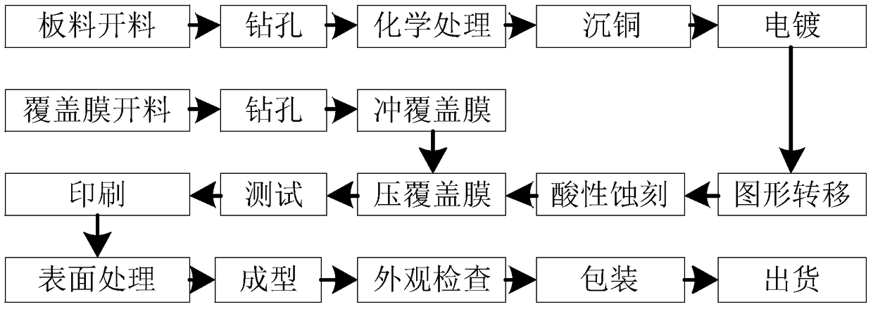
[0012] Please refer to figure 1 , the invention provides a kind of production method of double-sided thick copper flexible working plate, comprising:

[0013] Step 1, Drilling: Use a diamond-coated drill with a cutting speed of 1-2m / min, a cutting speed of 10-12m / min, a speed of 20KRPM, a cutting amount of 0.05-0.1mm / circle, and 500-1000 Hole / branch drill life, 2-4PNL / stack number of stacked boards to drill through holes on the substrate; using these parameters to produce, can effectively control the roughness in the hole and board surface burrs, burrs and other problems, to ensure that the hole The substrate is intact and undamaged. In this process, the drilling quality should be strictly controlled. The roughness in the hole is not allowed to b...


PUM

PropertyMeasurementUnit
hardnessaaaaaaaaaa

Abstract

The invention provides a method for producing a double-surface thick copper flexible working board. The invention is characterized by comprising the steps of a first step, drilling; a second step, chemical treatment; a third step, copper deposition; a fourth step, electroplating; a fifth step, pattern transferring; a sixth step, acid etching; a seventh step, covering film pressure-overlying, wherein the seventh step comprises procedures of A, treating a copper surface by means of a copper surface coarsening solution for etching the copper surface to a coarse surface and forming a honeycomb-shaped surface, B, in performing covering film pressure-overlying, utilizing silicone rubber with hardness of 45+ / -5 DEG C and temperature resistance of 250 DEG C above and below the substrate as accessories for ensuring high pressure overlaying effect of the covering film, and C, at a press jointing temperature of 190-200 DEG C and a press jointing pressure of 10-15Kg / m<2>, performing press jointing for 2-4 minutes, thereby jointing the substrate with the covering film for obtaining the working board. Because the technical solution is used, the method for producing the double-surface thick copper flexible working board has advantages of simple process, low cost, high drilling quality, and electroplating uniformity. The method further prevents the problems of bubbles on the covering film, filling glue insufficiency, thermal shock and laying in a reflow soldering test.

Description

technical field [0001] The invention relates to the field of circuit board production, in particular to a production method for a double-sided thick copper flexible working board. Background technique [0002] At present, the surface copper thickness of the flexible working board is generally 35um, and the hole copper is generally ≥12um. The process is relatively simple and the process is easy to control. However, when the conventional process is used to produce thick copper (such as surface copper thickness ≥ 70um), it will be quite difficult, and some problems cannot even be solved, as follows: [0003] (1) Problems such as drilling burrs, large roughness in the hole, and hole deformation; (2) Poor plating uniformity, uneven plate thickness, residual copper on the edge of the plate or small line spacing during etching; (3) Pressed cover film There is color difference, poor appearance, and at the same time, there will be insufficient glue filling at the line gap position, ...

Claims


Application Information

Patent Timeline
Patent Type & Authority Patents(China)
IPC IPC(8): H05K3/00
CPCH05K3/0044H05K2203/06H05K2203/0723H05K2203/0789
Inventor 陈荣贤陈启涛贺培严程有和
Owner 恩达电路(深圳)有限公司
Why Eureka
Try Eureka