
Solder mask preparing method for thick copper plates

A technology of thick copper plate and solder resist, which is applied in the field of solder resist preparation of PCB boards and thick copper plates, can solve the problems of long production process and low production efficiency, and achieve significant cost reduction, process length reduction and quality improvement significant effect

Inactive Publication Date: 2015-11-18
江西景旺精密电路有限公司
View PDF3 Cites 6 Cited by
  • Summary
  • Abstract
  • Description
  • Claims
  • Application Information

AI Technical Summary

Problems solved by technology

The production efficiency is extremely low, the production process is long, and it is easy to cause quality problems.

Method used

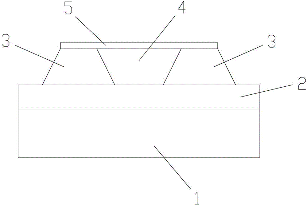

Image

  • Solder mask preparing method for thick copper plates

Examples


Embodiment 1

[0022] In an embodiment of the present invention, a method for preparing a solder resist of a thick copper plate comprises the following steps:

[0023] A. Use mixed water brown corundum with a volume ratio of 1:5 and a particle size of 180# to spray the circuit surface of the thick copper plate, and the spray pressure is not less than 3kg / cm 2 , The speed of the whole line is 30% of the 1oz thick copper plate, to clean the surface of the thick copper plate and roughen the copper layer to ensure the quality of line processing;

[0024] B. Filling resin with optional viscosity between 160-180dpa.s, resin content of 90wt%-95wt%, and filler content of 5wt%-10wt% is used to print the circuit layer of the thick copper plate with a conventional 18T inclined screen filling;

[0025] C. After vacuuming for 0.5H, place the thick copper plate at 150°C and bake for 15 minutes to cure the filling resin;

[0026] D. Use 500# non-woven cloth brush to eliminate glue overflow on the circuit...

Embodiment 2

[0029] In an embodiment of the present invention, a method for preparing a solder resist of a thick copper plate comprises the following steps:

[0030] A. Use mixed water brown corundum with a volume ratio of 1:5 and a particle size of 180# to spray the circuit surface of the thick copper plate, and the spray pressure is not less than 3kg / cm 2 , The speed of the whole line is 30% of the 1oz thick copper plate, to clean the surface of the thick copper plate and roughen the copper layer to ensure the quality of line processing;

[0031] B, alternative viscosity is 160dpa.s, resin content is 90wt%, filler content is at the filling resin of 10wt%, uses conventional 18T inclined screen to print and fill the circuit layer that thick copper board obtains;

[0032] C. After vacuuming for 0.5H, place the thick copper plate at 150°C and bake for 15 minutes to cure the filling resin;

[0033] D. Use a 500# non-woven cloth brush to eliminate the glue overflow on the circuit surface on t...

Embodiment 3

[0036] In an embodiment of the present invention, a method for preparing a solder resist of a thick copper plate comprises the following steps:

[0037] A. Use mixed water brown corundum with a volume ratio of 1:5 and a particle size of 180# to spray the circuit surface of the thick copper plate, and the spray pressure is not less than 3kg / cm 2 , The speed of the whole line is 30% of the 1oz thick copper plate, to clean the surface of the thick copper plate and roughen the copper layer to ensure the quality of line processing;

[0038] B, alternative viscosity between 180dpa.s, resin content of 95wt%, filler content of 10wt% filling resin, use conventional 18T inclined screen to print and fill the circuit layer obtained from the thick copper plate;

[0039] C. After vacuuming for 0.5H, place the thick copper plate at 150°C and bake for 15 minutes to cure the filling resin;

[0040] D. Use a 500# non-woven cloth brush to eliminate the glue overflow on the circuit surface on th...


PUM


Abstract

The invention discloses a solder mask preparing method for thick copper plates, comprising the following steps: A, selecting a mixed abrasive to clean the surface of a thick copper plate and coarsening a copper layer; B, preparing filling resin of which the viscosity is 160-180dpa.s, and using a conventional 18T slope screen to fill a circuit layer of the thick copper plate through printing; C, after extracting 0.5 H of vacuum, pre-baking the thick copper plate to cure the filling resin; D, using a nonwoven abrasive brush to remove excessive glue on the circuit surface of the thick copper plate; and E, carrying out a solder mask manufacturing process in a conventional mode based on the copper thickness of 1oz. By adopting the method to prepare the solder mask, for a thick copper plate with the copper thickness of 4-10oz, the number of times of solder mask manufacturing can be effectively reduced, and the length of the process can be reduced greatly. The method has a significant positive effect on cost reduction and quality improvement.

Description

technical field [0001] The invention belongs to the technical field of PCB production, and in particular relates to a solder resist preparation method for a thick copper plate, in particular to a solder resist preparation method for a PCB board with a surface copper foil thickness of 4-10 oz. Background technique [0002] Compared with the traditional PCB board, the heat dissipation advantage of the metal substrate makes it more popular in high-power applications. As the thermal conductivity and voltage resistance of the dielectric layer are getting better and better, the thickness of the PCB wires used to carry high currents is getting more and more thick. High, the difficulty of corresponding solder mask production is also getting higher and higher. The production efficiency is extremely low, the production process is long, and quality problems are easily caused by the multiple production mode of layered printing used in the production of thick copper metal substrate solde...

Claims


Application Information

Patent Timeline
Patent Type & Authority Applications(China)
IPC IPC(8): H05K3/28
CPCH05K3/28H05K2203/025H05K2203/0759
Inventor 肖世翔
Owner 江西景旺精密电路有限公司
Learn More