
A kind of semiconductor device and its preparation method, electronic device

A semiconductor and device technology, applied in the field of semiconductor devices and their preparation, can solve the problems of rough slope profile, unfavorable process, difficult and other problems, and achieve the effect of improving performance and surface roughness

Active Publication Date: 2018-05-08
SEMICON MFG INT (SHANGHAI) CORP
View PDF4 Cites 0 Cited by
  • Summary
  • Abstract
  • Description
  • Claims
  • Application Information

AI Technical Summary

Problems solved by technology

[0003] In 3D integrated circuits, patterning is usually performed on slopes to form various patterns. In this patterning step, slopes with mild gradients are usually selected. For example, the acute angle formed between the slope and the horizontal plane is 30- 40°, but most of the current methods for preparing slopes have the problem of inaccurate angles. It is difficult to obtain 30-40° slopes by conventional etching methods. For example, the acute angle between the slopes prepared by conventional dry etching methods and the horizontal plane is 50° °, and the profile of the prepared slope is rough, which is not conducive to the subsequent process

Method used


Image

  • A kind of semiconductor device and its preparation method, electronic device
  • A kind of semiconductor device and its preparation method, electronic device
  • A kind of semiconductor device and its preparation method, electronic device

Examples


preparation example Construction

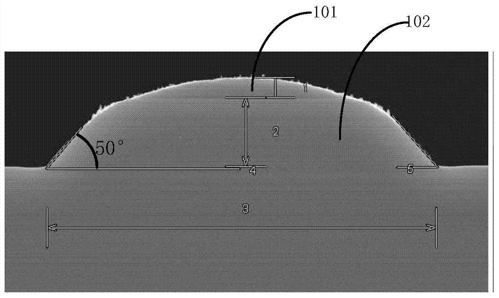
[0051]There are currently two methods for preparing slopes in semiconductor devices: the first one is to provide a base 102, and then form a patterned photoresist 101 on the base, the photoresist layer has a tapered profile, and then the The pattern is transferred to the substrate 102. The second method is to provide the substrate, then use dry etching, and adjust the parameters in the dry etching process to obtain the target slope, but the above two methods have disadvantages, such as the target slope The acute angle formed with the horizontal plane is 30-40°, but the acute angle formed between the slope prepared by the above two methods and the horizontal plane is about 50°, such as figure 1 As shown, it is difficult to achieve the target angle, the process is difficult to control, and the prepared inclined surface is rough, which is not conducive to the subsequent process.

[0052] In order to obtain a slope with a gentler slope, the present invention eliminates the limitat...

Embodiment 1

[0056] Attached below Figure 2a-2e The method is described further.

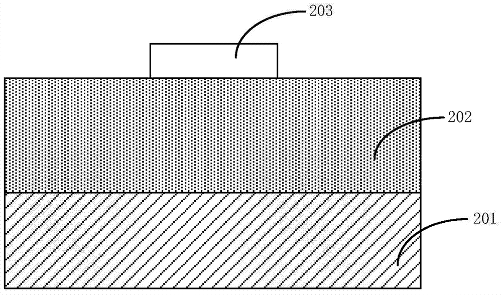
[0057] First, step 201 is performed to provide a semiconductor substrate 201 on which an oxide layer 202 is formed.

[0058] Specifically, such as Figure 2a As shown, the semiconductor substrate 201 may be at least one of the materials mentioned below: silicon, silicon-on-insulator (SOI), silicon-on-insulator (SSOI), silicon-germanium-on-insulator (S-SiGeOI ), silicon germanium on insulator (SiGeOI) and germanium on insulator (GeOI), etc.

[0059] In this embodiment, the semiconductor substrate 201 is made of silicon.

[0060] The oxide layer 202 is silicon oxide, but not limited to silicon oxide, the oxide mask layer can also be ZnO, CdO, TiO 2 、Al 2 o 3 , SnO, Cu 2 O, NiO, CoO, FeO, and Cr 2 o 3 One of.

[0061] Step 202 is executed to form a patterned mask layer 203 on the oxide layer 202 , and a stripe pattern is formed in the mask layer 203 .

[0062] Specifically, the mask layer 203 can be...

Embodiment 2

[0101] Attached below Figure 3a-3f The method is described further.

[0102] First, step 301 is performed to provide a semiconductor substrate 301 on which an oxide layer 302 is formed.

[0103] Specifically, such as Figure 3a As shown, the semiconductor substrate 301 may be at least one of the materials mentioned below: silicon, silicon-on-insulator (SOI), silicon-on-insulator (SSOI), silicon-germanium-on-insulator (S-SiGeOI ), silicon germanium on insulator (SiGeOI) and germanium on insulator (GeOI), etc.

[0104] In this embodiment, the semiconductor substrate 301 is silicon.

[0105] The oxide layer 302 is silicon oxide, but not limited to silicon oxide, the oxide mask layer can also be ZnO, CdO, TiO 2 、Al 2 o 3 , SnO, Cu 2 O, NiO, CoO, FeO, and Cr 2 o 3 One of.

[0106] Step 302 is executed to form a patterned mask layer 303 on the oxide layer 302 , and a stripe pattern is formed in the mask layer 303 .

[0107] Specifically, the mask layer 303 can be a mask ...


PUM


Abstract

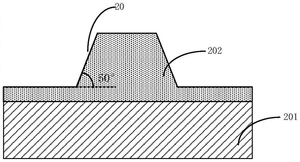
The present invention relates to a semiconductor device, its preparation method, and an electronic device. The method includes: providing a substrate, forming a protrusion having a first slope on the substrate, and the acute angle formed by the first slope and a horizontal plane is 50- 60°; a thin film layer is deposited on the protrusion to form a second slope on the first slope, and the acute angle formed between the second slope and the horizontal plane is 30-40°. The advantages of the present invention are: (1) The present invention breaks through the limitation of the 50-60° slope in the prior art, and prepares a slope with a gentler slope. (2) The inclined surface prepared by the method of the present invention is greatly improved by the deposition method compared with the inclined surface obtained by etching, which is beneficial to the subsequent process and further improves the performance of the semiconductor device.

Description

technical field [0001] The present invention relates to the field of semiconductors, in particular, the present invention relates to a semiconductor device, a preparation method thereof, and an electronic device. Background technique [0002] In the field of semiconductors, multi-function devices are becoming more and more popular among consumers. Compared with devices with simple functions, the production process of multi-function devices will be more complicated. For example, multiple chips with different functions need to be integrated on the circuit board. 3D integrated circuit (integrated circuit, IC) technology, 3D integrated circuit (integrated circuit, IC) is defined as a system-level integration structure, stacking multiple chips in a vertical direction, thereby saving space. [0003] In 3D integrated circuits, patterning is usually performed on slopes to form various patterns. In this patterning step, slopes with mild gradients are usually selected. For example, th...

Claims


Application Information

Patent Timeline
Patent Type & Authority Patents(China)
IPC IPC(8): H01L21/02H01L21/027
Inventor 倪梁汪新学伏广才
Owner SEMICON MFG INT (SHANGHAI) CORP
Learn More