Chip packaging structure and manufacture method thereof, and chip packaging substrate

A technology of chip packaging structure and manufacturing method, which is applied in semiconductor/solid-state device manufacturing, electrical components, electrical solid-state devices, etc., can solve the problems of insufficient welding height, the chip cannot be firmly packaged, and the diameter of the solder ball becomes smaller. The effect of improving welding yield

Inactive Publication Date: 2015-11-25
QI DING TECHNOLOGY QINHUANGDAO CO LTD +1
View PDF4 Cites 5 Cited by
  • Summary
  • Abstract
  • Description
  • Claims
  • Application Information

AI Technical Summary

Problems solved by technology

Under the demand of high-density wiring, the line is getting thinner and thinner, and the opening of the solder mask is getting smaller and smaller, so the size of the pad defined by the opening of the solder mask is getting smaller and smaller, so that poor soldering occurs frequently. On the one hand, solder balls are not easy to fill into the opening of the solder mask, which will cause empty soldering. On the other hand, the diameter of the solder ball becomes smaller as the size of the solder mask opening becomes smaller, so that the soldering height is insufficient, resulting in a gap between the chip and the package substrate. The distance is not enough, it is difficult to fill the encapsulant, which leads to the fact that the chip cannot be firmly packaged on the package substrate

Method used


Image

  • Chip packaging structure and manufacture method thereof, and chip packaging substrate
  • Chip packaging structure and manufacture method thereof, and chip packaging substrate
  • Chip packaging structure and manufacture method thereof, and chip packaging substrate

Examples


Embodiment Construction

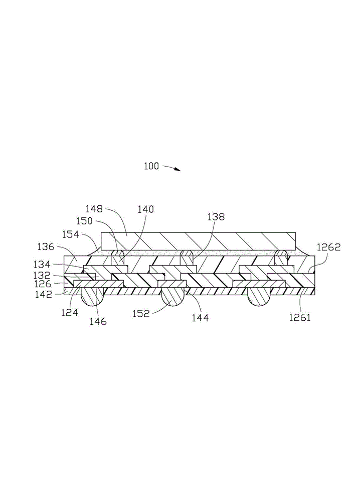
[0055] see figure 1 , the first embodiment of the present invention provides a chip packaging structure 100, including: a first dielectric layer 126, the first dielectric layer 126 includes a first surface 1261 and a second surface 1262 opposite; a first conductive Circuit layer 124, the first conductive circuit layer 124 is formed on the first surface 1261 of the first dielectric layer 126 and embedded in the first dielectric layer 126, and the first conductive circuit layer The surface of 124 away from the second surface 1262 is flush with the first surface 1261; a second conductive circuit layer 134, the second conductive circuit layer 134 is formed on the second surface 1262, the second The conductive circuit layer 134 is electrically connected to the first conductive circuit layer 124 through a plurality of first conductive columns 132; a second dielectric layer 136, the second dielectric layer 136 is formed on the second surface 1262 and On the surface of the second con...


PUM


Abstract

A manufacturing method of a chip packaging structure comprises the steps that a loading plate is provided, a first conductive line layer, a first dielectric layer and a second conductive line layer are successively formed at one side at least of the loading plate, and the first conductive line layer is connected with the second conductive line layer via first conductive poles; a second dielectric layer is formed at one side, far from the loading plate, of the second conductive line layer, openings of the second dielectric layer are formed in the second conductive dielectric layer, and form second conductive poles via electroplating, the second conductive line layer is electrically connected with the second conductive poles, and the surfaces, far from the first dielectric layer, of the second conductive poles are approximately leveled with the surface, far from the first dielectric layer, of the second dielectric layer; and the loading plate is removed, and a chip is welded to form the chip packaging structure. The invention also relates to a chip packaging substrate and structure.

Description

technical field [0001] The invention relates to the field of circuit board manufacturing, in particular to a chip packaging structure, a manufacturing method and a chip packaging substrate. Background technique [0002] The chip packaging substrate can provide the chip with electrical connection, protection, support, heat dissipation, assembly and other functions to achieve multi-pin, reduce the size of packaged products, improve electrical performance and heat dissipation, ultra-high density or multi-chip modularization. Generally, the chip packaging substrate forms an opening in the solder resist layer on the side where the chip is placed, so as to expose the solder pads, so that solder balls can be formed on the surface of the solder pads and soldered to the chip. Under the demand of high-density wiring, the line is getting thinner and thinner, and the opening of the solder mask is getting smaller and smaller, so the size of the pad defined by the opening of the solder ma...

Claims


Application Information

Patent Timeline
Patent Type & Authority Applications(China)
IPC IPC(8): H01L21/48H01L21/60H01L23/498
CPCH01L2224/73204
Inventor 李嘉伟
Owner QI DING TECHNOLOGY QINHUANGDAO CO LTD
Why Eureka
Try Eureka