Measurement method, etching method and formation method of semiconductor device

A semiconductor and dry etching technology, which is applied in the measurement method, etching method and formation field of semiconductor devices, can solve the problems of inaccurate optical measurement of key dimensions of semiconductor devices, improve process control capabilities, save high costs, Solve the effect of inaccurate measurement

Active Publication Date: 2018-04-13
CSMC TECH FAB2 CO LTD
View PDF3 Cites 0 Cited by
  • Summary
  • Abstract
  • Description
  • Claims
  • Application Information

AI Technical Summary

Problems solved by technology

[0005] In view of the above-mentioned shortcomings of the prior art, the object of the present invention is to provide a measurement method, an etching method and a forming method of a semiconductor device, so as to solve the problem of semiconductor devices caused by dry etching using an organic anti-reflection layer as an etching barrier layer in the prior art. The problem of inaccurate critical dimension optical measurement (CD measurement)

Method used


Image

  • Measurement method, etching method and formation method of semiconductor device
  • Measurement method, etching method and formation method of semiconductor device

Examples


Embodiment Construction

[0024] Embodiments of the present invention are described below through specific examples, and those skilled in the art can easily understand other advantages and effects of the present invention from the content disclosed in this specification. The present invention can also be implemented or applied through other different specific implementation modes, and various modifications or changes can be made to the details in this specification based on different viewpoints and applications without departing from the spirit of the present invention.

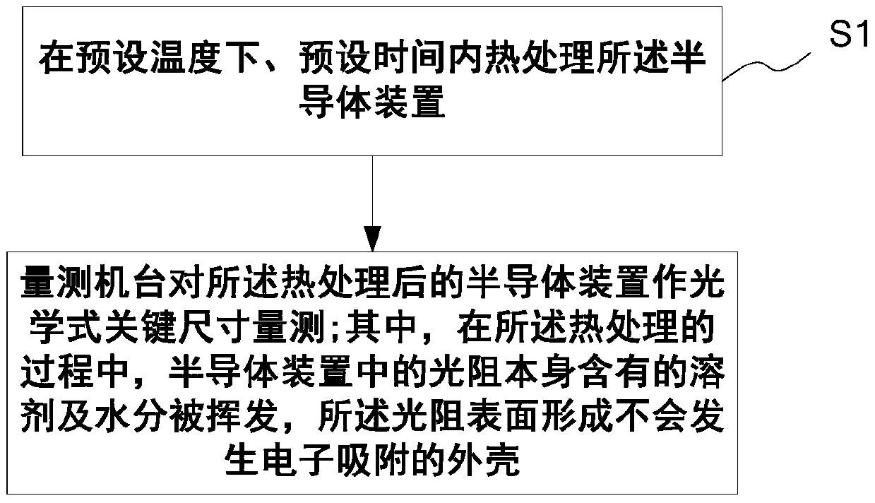
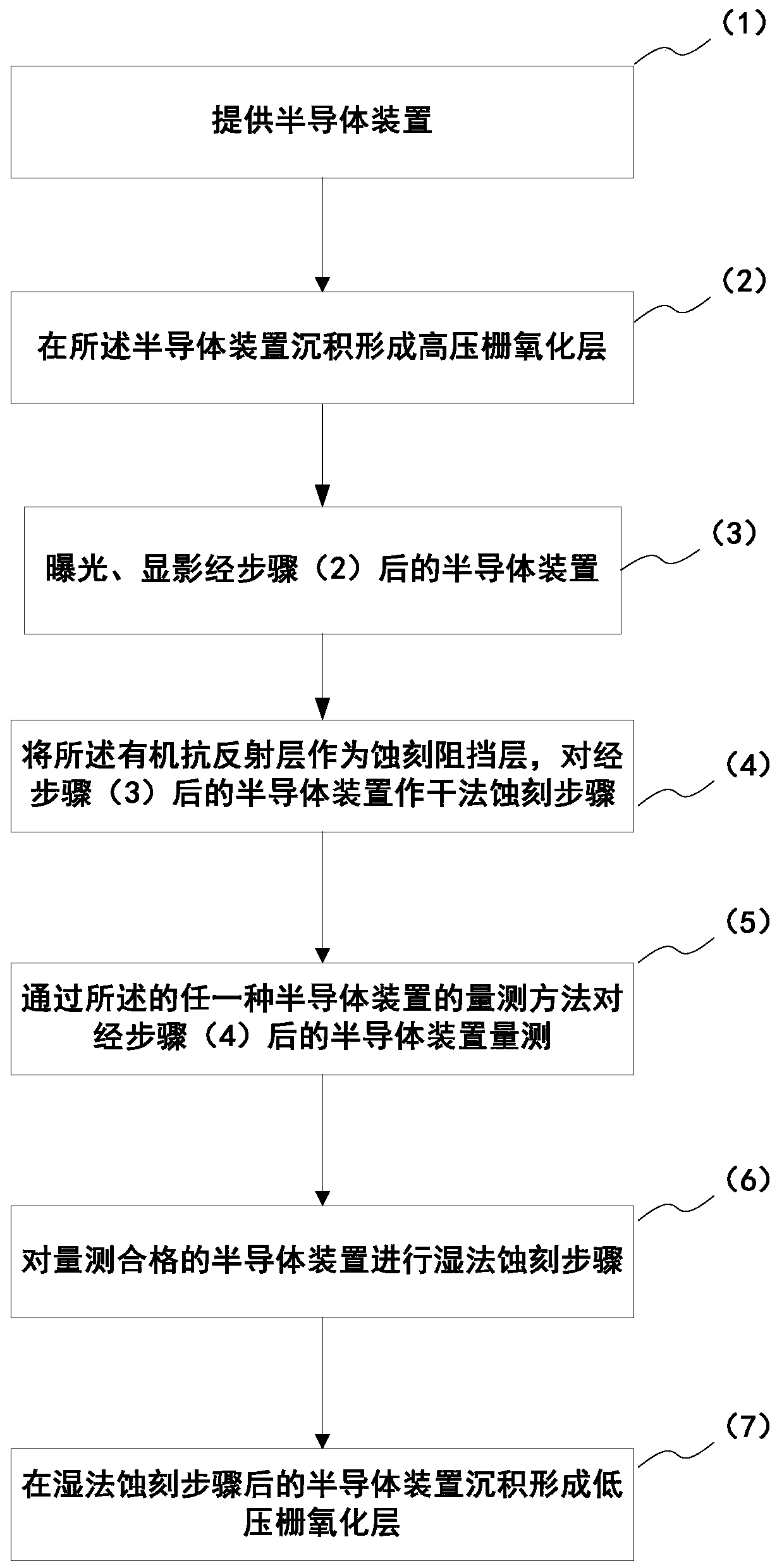
[0025] see figure 1 , a method for measuring a semiconductor device provided by the present invention, wherein the semiconductor device is obtained by performing dry etching with an organic anti-reflection layer (Barc) as an etching barrier layer. In this embodiment, the etching is a technique of removing materials by chemical reaction or physical impact. Etching techniques can be classified into wet etching and dry etching.

[0026...


PUM


Abstract

The invention provides a measuring method, etching method, and forming method of a semiconductor device. The semiconductor device is obtained by performing Barc Open on an organic antireflective layer used as a mask. According to the measuring method, the semiconductor device is subjected to thermal treatment within preset time and at a preset temperature and a measuring machine performs optical critical dimension measurement on the semiconductor device having been subjected to the thermal treatment, wherein in the thermal treatment process, the solvent and the water that are contained in a photoresistor in the semiconductor device volatilize and a housing is formed in the surface of the photoresistor and cannot generate electron absorption. The housing formed in the surface of the semiconductor device having been subjected to the thermal treatment is relatively hard and smooth and prevents a phenomenon of electron absorption such that optical critical dimension measurement is clear and accurate. As a result, a problem of inaccurate measurement is solved fundamentally; wafer verification is prevented; a process management and control capability is greatly improved; and high cost is saved.

Description

technical field [0001] The invention relates to the technical field of semiconductor packaging equipment, in particular to a measuring method, an etching method and a forming method of a semiconductor device. Background technique [0002] Using the organic anti-reflective layer as a mask (ie, etch barrier layer) for dry etching (Barc Open) as a key process step for forming a low-voltage gate oxide layer (LV oxide) for a dual gate (Dual Gate) device, its critical dimension (CD) Measurement is very important for process control, but since the wafer is directly measured for CD after dry etching without dry debonding and wet cleaning, the surface of the wafer (wafer) continues to accumulate under electron beam irradiation. The charge repulses the electron beam, which eventually causes the surface of the wafer to be out of focus under the lens, the measuring machine cannot distinguish the measurement pattern, and the CD measurement cannot obtain the correct value. [0003] Takin...

Claims


Application Information

Patent Timeline
Patent Type & Authority Patents(China)
IPC IPC(8): H01L21/66H01L21/28H01L27/115
Inventor 周耀辉
Owner CSMC TECH FAB2 CO LTD
Why Eureka
Try Eureka