Two-way photosensitive thyristor chip and solid-state relay (SSR)
A thyristor, bidirectional light technology, applied in circuits, electrical components, semiconductor devices, etc., can solve problems such as efficiency performance/cost deterioration, minimize inventory, reduce the number of parts, and avoid the effects of high-variety and low-volume production
- Summary
- Abstract
- Description
- Claims
- Application Information
AI Technical Summary
Problems solved by technology
Method used
Image
Examples
no. 1 approach
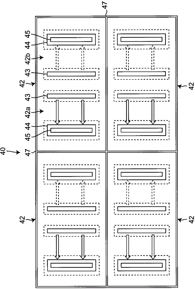
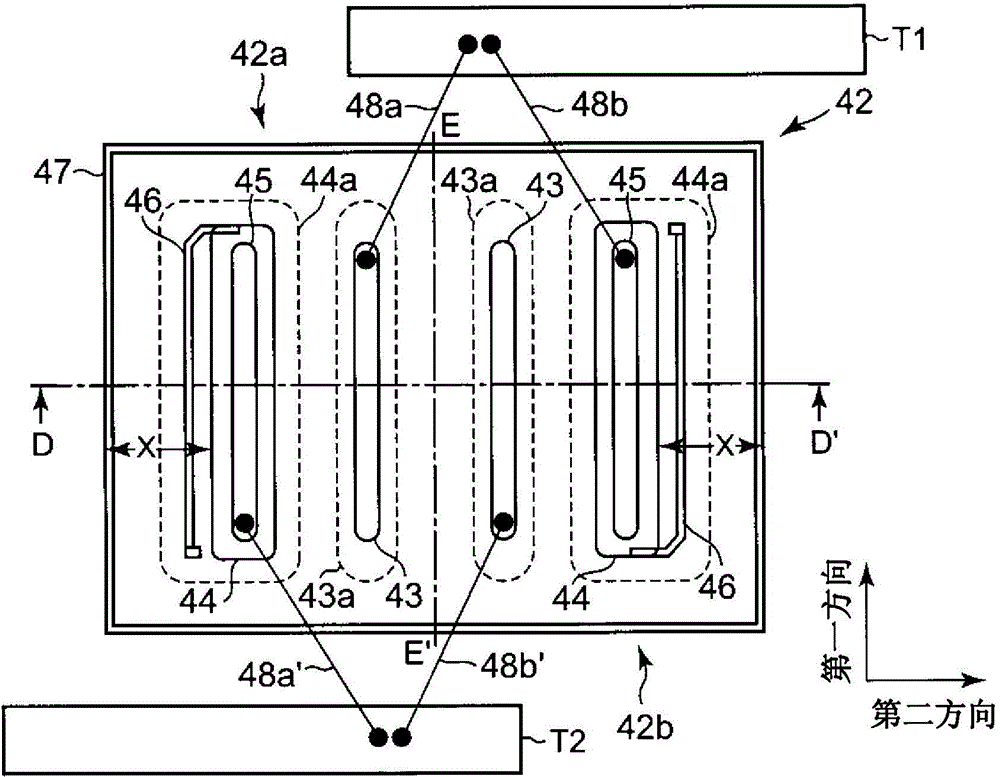
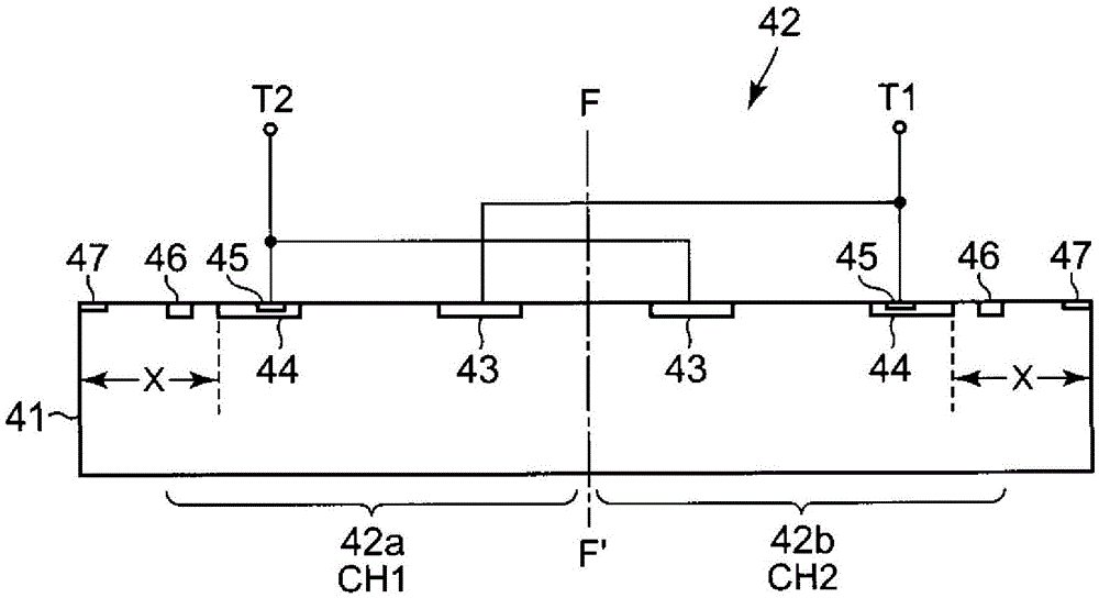
[0099] figure 1A schematic pattern layout in the bidirectional photothyristor chip of this embodiment is shown. The bidirectional photothyristor chip 40, such as Figure 15 In the bidirectional photothyristor chip disclosed in the above-mentioned Patent Document 1, the photothyristor chip including CH1 and the photothyristor CH2 will have a point-symmetrical pattern with respect to the center line and the intersection point of a line perpendicular to the center line. When the bidirectional photothyristor is defined as the cell 42 which is the minimum unit, an arbitrary number of cells 42 are mounted on one semiconductor chip. Here, the first photothyristor 42 a of CH1 and the second photothyristor 42 b of CH2 have an anode diffusion region 43 , a gate diffusion region 44 and a cathode diffusion region 45 . In addition, arrows indicate the flow direction of electric current.
[0100] In this bidirectional photothyristor chip 40 , a plurality of units 42 composed of the abov...
no. 2 approach
[0138] Figure 9 The wiring structure of the above-mentioned cells in the bidirectional photothyristor chip of this embodiment is shown. This bidirectional photothyristor chip 40 is the same as the case of the above-mentioned first embodiment, and is equipped with any number of CH1 including CH1 having a pattern point-symmetrical with respect to the intersection point of the center line and a line perpendicular to the center line. A photothyristor 42a of CH2 and a second photothyristor 42b of CH2 form the unit 42 of the bidirectional photothyristor.
[0139] In the above-mentioned first embodiment, among the bidirectional photothyristors constituting the unit 42, the first photothyristor 42a of CH1 and the second photothyristor 42b of CH2 are wired in antiparallel through the lead frame T1 and the lead frame T2. Therefore, the first photothyristor 42a of CH1 and the second photothyristor 42b of CH2 are triggered alternately, and are used for bidirectional AC operation from le...
no. 3 approach
[0145] Figure 10 The wiring structure between the said cells in the bidirectional photothyristor chip of this embodiment is shown. The bidirectional photothyristor chip 40 of the present embodiment is composed of two cells (bidirectional photothyristors) 42 . In each cell 42, the anode diffusion region 43 of the first photothyristor 42a of CH1 and the cathode diffusion region 45 of the second photothyristor 42b of CH2 are connected to each other by the internal wiring 53, as in the first embodiment described above. In addition, the cathode diffusion region 45 of the first photothyristor 42 a of CH1 and the anode diffusion region 43 of the second photothyristor 42 b of CH2 are connected to each other by an internal wiring 54 .
[0146] In addition, among the two cells (bidirectional photothyristors) 42, the Al electrode 43a on the anode diffusion region 43 of the first photothyristor 42a of CH1 is connected to the lead frame T2 via Au wires 55a and 55b. In addition, the Al e...
PUM
 Abstract
Description
Claims
Application Information
 - R&D
- Intellectual Property
- Life Sciences
- Materials
- Tech Scout
- Unparalleled Data Quality
- Higher Quality Content
- 60% Fewer Hallucinations
Browse by: Latest US Patents, China's latest patents, Technical Efficacy Thesaurus, Application Domain, Technology Topic, Popular Technical Reports.
© 2025 PatSnap. All rights reserved.Legal|Privacy policy|Modern Slavery Act Transparency Statement|Sitemap|About US| Contact US: help@patsnap.com


