Driver circuit for power control

A driving circuit and power control technology, applied in the field of driving circuits for power control, can solve the problems of unsatisfactory working state of a controlled power control device, complicated control signal processing circuit, etc.

Inactive Publication Date: 2017-12-15
盐城咏恒投资发展有限公司
View PDF6 Cites 0 Cited by
  • Summary
  • Abstract
  • Description
  • Claims
  • Application Information

AI Technical Summary

Problems solved by technology

[0006] It can be seen that the control signal processing circuits of the P-NMOSFET combination in Figure 1(B) and the P-PMOSFET combination in Figure 1(C) are relatively complicated, especially during the dead zone protection time, the working state of the controlled power control device Q3 is not correct. ideal

Method used


Image

  • Driver circuit for power control
  • Driver circuit for power control
  • Driver circuit for power control

Examples


Embodiment 1

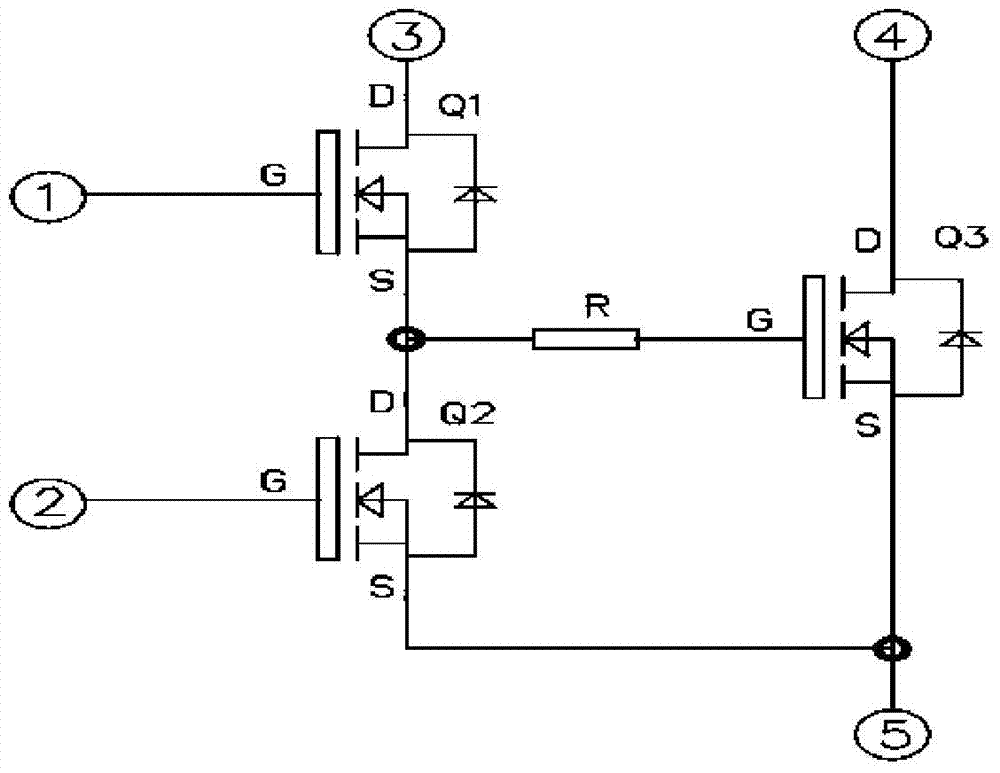
[0032] like figure 2 , the driving circuit for power control in this embodiment includes: the front stage of the driving circuit formed by the driving integrated circuit U1, which is used to control the output voltage of its voltage output terminal OUT according to the PWM signal (or logic signal) sent in from the outside; N- MOSFET (Q1), its gate G is connected to the voltage output terminal OUT of the driving integrated circuit; a first resistor R1 is set between the gate G of the N-MOSFET (Q1) and the original electrode S, and the N-MOSFET (Q1 )’s drain D is connected to the driving power supply; the gate G of the P-MOSFET (Q2) is connected to the voltage output terminal OUT of the driving integrated circuit; the source S of the N-MOSFET (Q1) is connected to the P-MOSFET (Q2 ) between the sources S of the second resistor R2; the controlled power control device Q3, the gate G of which is connected in series with the third resistor R3 and then connected to the source S of the...

Embodiment 2

[0039] On the basis of Embodiment 1, the drive circuit for power control in this embodiment has the following modifications:

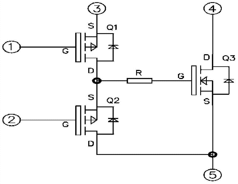
[0040] like image 3 , the voltage output terminal OUT of the driving integrated circuit is sequentially connected in series with the fourth resistor R4, the fifth resistor R5 and the first gate resistor RG1, and then connected to the gate G of the N-MOSFET (Q1); the fifth resistor R5 and The contact of the first gate resistor RG1 is connected in series with the first resistor R1 and then connected to the original electrode S of the N-MOSFET (Q1); the contacts of the fourth resistor R4 and the fifth resistor R5 are connected in series with the second gate resistor RG2 and then connected Gate G of the P-MOSFET (Q2).

[0041] Pin 3 is connected to the drive power. When the controlled power control device Q3 is used for the upper bridge, pin 4 is connected to the power supply positive of the power stage, and pin 5 is the output. When the controlled pow...

Embodiment 3

[0054] On the basis of Embodiment 1, the front stage of the driving circuit of this embodiment adopts Figure 8 The structure of the split devices shown is specifically adopted Figure 8 The front stage of the driving circuit is formed by the array devices on the left side of the dotted line.

[0055] Figure 8 Among them, pins 1 and 5 are connected to the drive power supply, generally 12V~15V.

[0056] Pin 2 is the input of the upper bridge control signal PWM (or logic signal).

[0057] Pin 7 is the input of the lower bridge control signal PWM (or logic signal).

[0058] Pin 6 is connected to the positive pole of the logic power supply, usually 3.3V or 5V.

[0059] Pin 8 is connected to the positive pole of the power supply.

[0060] Pin 10 is connected to the negative pole of the power supply.

[0061] Pin 9 is the power output.

[0062]D11 and C11 form a bootstrap boost circuit to provide drive power for the upper bridge.

[0063] The front stage of the drive circui...


PUM


Abstract

The invention relates to a drive circuit for power control which makes a switch-on time and a turn-off time of a controlled power controller (a Metal-Oxide-Semiconductor Field-Effect Transistor (MOSEFT) or an Insulated Gate Bipolar Transistor (IGBT)) short and makes a drive current enough large. The drive circuit for power control includes: a drive circuit pre-stage for controlling an output voltage at a voltage output terminal according to an externally sent Pulse Width Modulation (PWM) signal or a logic signal; an N-MOSFET, wherein a gate of the N-MOSFET is connected to the voltage output terminal of the drive circuit pre-stage, a first resistor is arranged between the gate and a source electrode of the N-MOSFET, and a drain electrode of the N-MOSFET is connected to a drive power supply; a P-MOSFET, wherein the gate of the P-MOSFET is connected to the voltage output terminal of a driving integrated circuit, a second resistor is arranged between the source electrode of the N-MOSFET and the source electrode of the P-MOSFET; and the controlled power controller, wherein the gate of the controlled power controller is connected to the source electrode of the P-MOSFET after serially connected with a third resistor, and the source electrode of the controlled power controller is connected to the drain electrode of the P-MOSFET.

Description

technical field [0001] The invention relates to a drive circuit for power control, especially a drive circuit for power control devices (MOSFET, IGBT, etc.) of power control equipment. The drive circuit can output peak current with larger amplitude and shorter rising and falling edges. The drive circuit can be applied to power control fields such as motor control, power conversion and power management using MOSFET and IGBT. Background technique [0002] In the prior art, when turning on a controlled power control device such as MOSFET or IGBT, the drive circuit must be able to inject a large current into the gate of the controlled power control device MOSFET or IGBT in a short time, and turn off the controlled power control device MOSFET or IGBT. , the driving circuit must be able to draw a large current from the gate of the controlled power control device MOSFET or IGBT in a short time. In other words, the driving current pulse amplitude applied to the gate of the control...

Claims


Application Information

Patent Timeline
Patent Type & Authority Patents(China)
IPC IPC(8): H03K17/687
CPCH02M1/088H03K17/687
Inventor 严舒
Owner 盐城咏恒投资发展有限公司
Why Eureka
Try Eureka