A device for nano-imprinting of a large-sized wafer and its imprinting method

A nanoimprint, large-scale technology, applied in the field of micro-nano manufacturing, to achieve the effect of eliminating bubble defects, high efficiency and low defects

Active Publication Date: 2019-08-13
兰红波
View PDF8 Cites 0 Cited by
  • Summary
  • Abstract
  • Description
  • Claims
  • Application Information

AI Technical Summary

Problems solved by technology

[0005] The purpose of the present invention is to solve the problem of large-size wafer-level micro-nano patterning, provide a device and method for nano-imprinting of large-size wafers, and realize high-efficiency and low-cost wafer processing on large-size substrates level graphics

Method used


Image

  • A device for nano-imprinting of a large-sized wafer and its imprinting method
  • A device for nano-imprinting of a large-sized wafer and its imprinting method
  • A device for nano-imprinting of a large-sized wafer and its imprinting method

Examples


Embodiment Construction

[0062] The technical solutions in the embodiments of the present invention will be clearly and completely described below in conjunction with the drawings in the embodiments of the present invention.

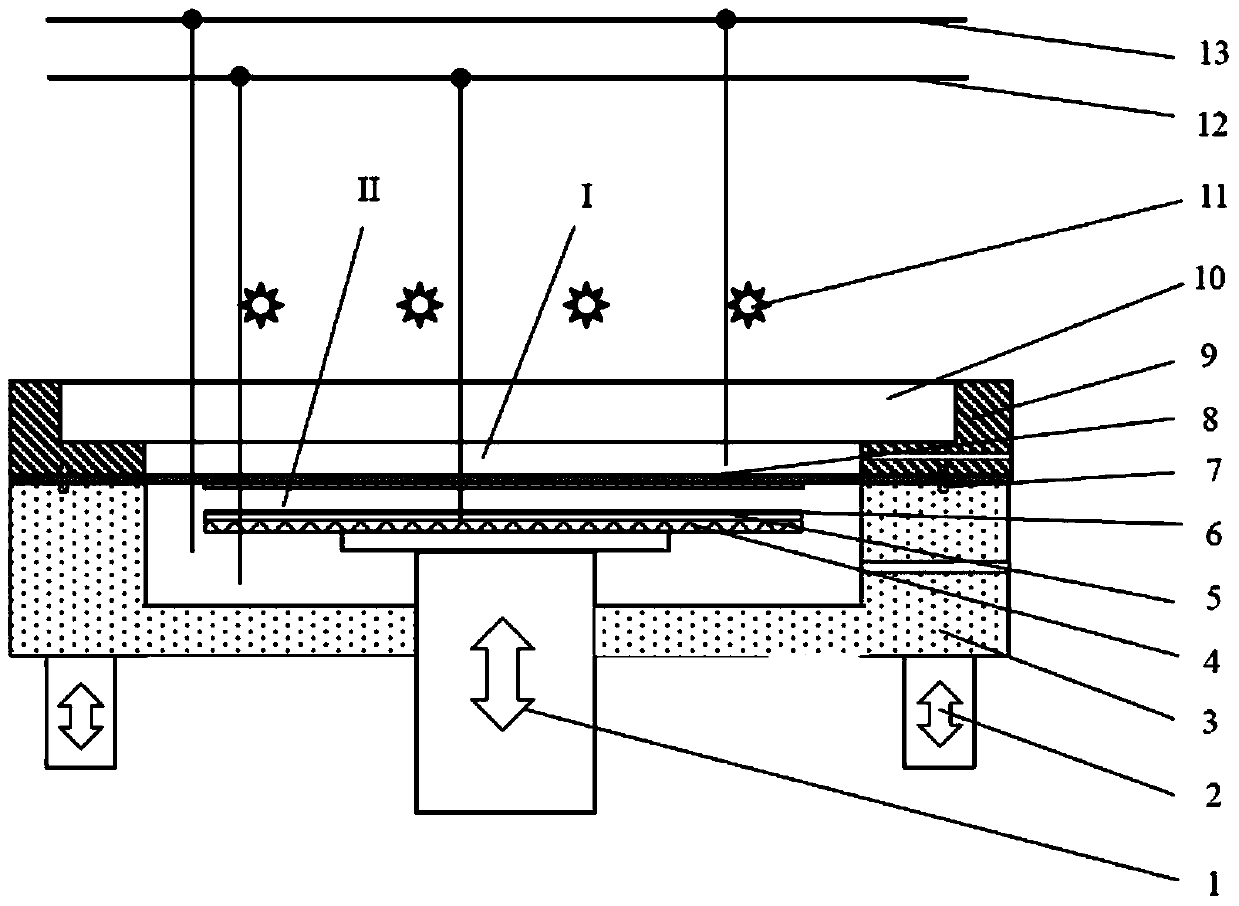
[0063] figure 1 It is a structural schematic diagram of the nano-imprinting device for a large-sized wafer of the present invention, which includes: a second lifting mechanism 1, a first lifting mechanism 2, a lower cavity 3, a wafer carrier 4, a wafer 5, an imprinting material 6, Sealing ring 7, mold 8, upper cavity 9, transparent glass (quartz glass) 10, exposure light source 11, vacuum pipeline 12, pressure pipeline 13; wherein, the workbench is placed at the bottom of the center of the device, and the workbench wears Through the lower cavity 3, the inside of the workbench is provided with a second lifting mechanism, and the carrier table 4 is horizontally placed inside the lower cavity 3; The bottom is connected; the wafer holder 4 is placed on the workbench; the wafer 5 is...


PUM

PropertyMeasurementUnit
thicknessaaaaaaaaaa
thicknessaaaaaaaaaa
thicknessaaaaaaaaaa

Abstract

A large-size wafer entire nanoimprinting device and an imprinting method therefor. The device comprises an upper cavity (9) and a lower cavity (3), the lower cavity (3) being driven by a first raising and lowering mechanism (2) to move up and down to come into contact with or be separated from the upper cavity (9), an elastic mould (8) used for imprinting being arranged on a bottom portion of the upper cavity (9), a wafer-bearing platform (4) being horizontally arranged within the lower cavity (3), a bottom portion of the wafer-bearing platform (4) being provided with a second raising and lowering mechanism (1), an upper cavity air inlet (902) movably connected to a pressure pipe (13) being arranged on a cavity wall of the upper cavity (9), a lower cavity air inlet (301) movably connected to both a vacuum pipe (12) and the pressure pipe (13) being arranged on a cavity wall of the lower cavity (3), a wafer-bearing platform air inlet in communication with the vacuum pipe (12) being arranged on the wafer-bearing platform (4), the device also comprising an exposure light source (11). The nanoimprinting device and the imprinting method therefor implement large-size, uneven substrate and fragile substrate large-area micro / nanostructure high-efficiency and low-cost batch manufacturing, and provide an industrial-grade solution for large-size wafer-level large-area micro / nanostructure manufacturing.

Description

technical field [0001] The invention relates to a device for nano-imprinting of a large-sized wafer and an imprinting method thereof, in particular to a method and device for mass-manufacturing large-area micro-nano structures with high efficiency and low cost, and belongs to the technical field of micro-nano manufacturing. Background technique [0002] Nanoimprint Lithography (NIL), as a new micro-nano manufacturing technology, has high resolution and ultra-low cost compared with the current projection lithography and next-generation lithography technology (evaluated by international authoritative organizations The level of NIL is at least an order of magnitude lower than that of traditional optical projection lithography) and high productivity, and its most significant advantages lie in the ability to manufacture large-area, complex three-dimensional micro-nano structures and the patterning of non-flat substrates, especially soft The UV nanoimprint process also has the pot...

Claims


Application Information

Patent Timeline
Patent Type & Authority Patents(China)
IPC IPC(8): G03F7/00
CPCG03F7/0002
Inventor 兰红波
Owner 兰红波
Why Eureka
Try Eureka