
A numerical simulation data processing method for a semiconductor device

A numerical simulation and data processing technology, applied in electrical digital data processing, special data processing applications, instruments, etc., can solve problems such as high cost of solving large linear equations, non-convergence of preprocessing technology solutions, and inability to meet industrial application requirements.

Active Publication Date: 2018-10-12
苏州培风图南半导体有限公司
View PDF4 Cites 0 Cited by
  • Summary
  • Abstract
  • Description
  • Claims
  • Application Information

AI Technical Summary

Problems solved by technology

[0011] The advantage of using the fully implicit method to solve: unconditionally stable, and limited to the time step; disadvantage: each time step needs to solve a large linear equation system, and each step has a large amount of calculation
For large asymmetric linear equation problems, the current iterative method mainly uses incomplete decomposition preprocessing techniques, such as ICC, ILU, but for some ill-conditioned problems, incomplete decomposition preprocessing techniques often lead to non-convergence of the solution
[0023] To sum up, the existing numerical simulation methods for semiconductor devices, that is, the numerical solution of equation group (2), cannot meet the existing industrial application requirements
The solution of the fully implicit method is unconditionally stable, but it has the disadvantage of high overhead for solving large linear equations
The existing iterative method for preprocessing of large linear equations is not suitable for solving linear equations of semiconductor numerical simulation, and further improvement is necessary

Method used


Image

  • A numerical simulation data processing method for a semiconductor device
  • A numerical simulation data processing method for a semiconductor device
  • A numerical simulation data processing method for a semiconductor device

Examples


Embodiment Construction

[0067] The specific implementation manners of the present invention will be further described in detail below in conjunction with the accompanying drawings and examples.

[0068] In the following, a method for processing numerical simulation data of a semiconductor device proposed by the present invention and establishing preconditioners for large linear equations in the fully implicit method are taken as a specific embodiment.

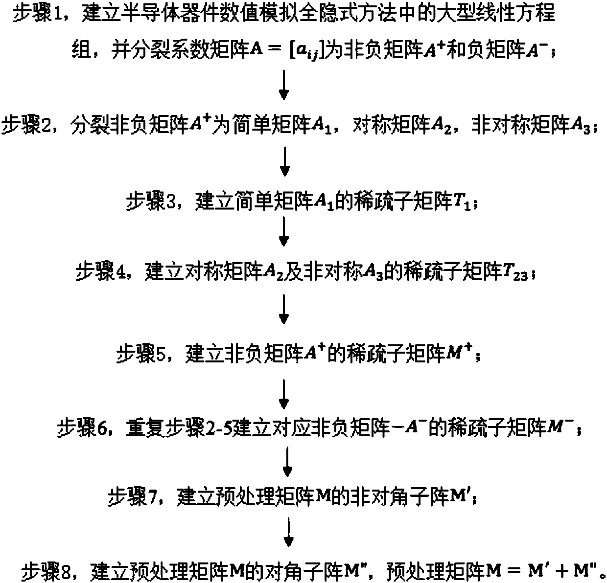
[0069] The schematic flow chart of the preprocessing method of the large-scale linear equation system of the semiconductor device numerical simulation that the present invention proposes is as figure 1 shown.

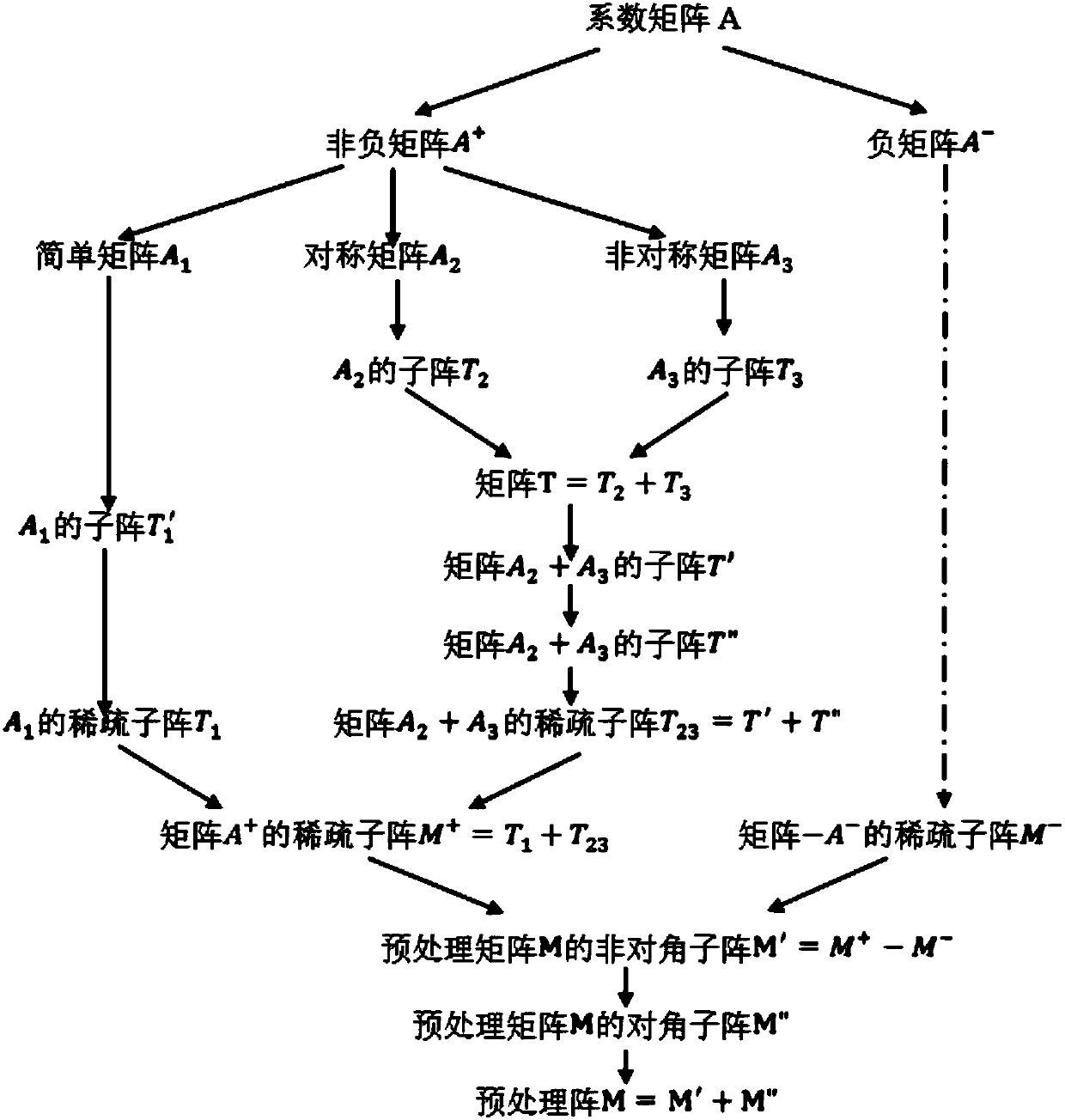
[0070] The schematic diagram of the matrix operation change of the establishment of the preconditioner proposed by the present invention is as follows figure 2 shown.

[0071]First, the preprocessing technology in the present invention is verified on a simple asymmetric linear equation system, and a specific embodiment of the simple asymmetr...


PUM


Abstract

The invention relates to a numerical simulation data processing method of a semiconductor device. The method is characterized by comprising the basic steps that 1, a large linear equation system of the semiconductor device in the numerical simulation total implicit method is built, and a coefficient matrix A=[aij] is split into a nonnegative matrix A<+> and a negative matrix A<->; 2, the nonnegative matrix A<+> is split into a simple matrix A1, a symmetric matrix A2 and a non-symmetric matrix A3; 3, a sparse submatrix T1 of the simple matrix A1 is built; 4, a sparse submatrix T23 of the symmetric matrix A2 and the non-symmetric matrix A3 is built; 5, a sparse submatrix M<+> of the nonnegative matrix A<+> is built; 6, the step 2 to the step 5 are repeatedly performed to build a sparse submatrix M<-> corresponding to the nonnegative matrix -A<->; 7, a non-diagonal submatrix M' of a preconditioning matrix M is built; 8, a diagonal submatrix M'' of the preconditioning matrix M is built, and the preconditioning matrix M =M'+M''. According to the preconditioning technology for building the large linear equation system, the corresponding equation system is small in calculating amount, high in precision and good in simulation stability, and therefore the numerical simulation total implicit method of the semiconductor device can meet the industrial application requirements.

Description

technical field [0001] The invention relates to the technical fields of microelectronics and semiconductors, in particular to a method for processing numerical simulation data of semiconductor devices. Background technique [0002] The rapid development of the electronic industry makes the performance of semiconductor devices more and more high, so the optimization of device structure by numerical simulation method has become an urgent problem to be solved. Numerical simulation of semiconductor devices is an important tool for analyzing the performance of semiconductor devices. [0003] Numerical simulation methods for semiconductor devices mainly include particle-based methods represented by Monte Carlo and continuum-based methods. The former directly solves the semiconductor Boltzmann transport equation, which has huge computational overhead, large statistical dispersion of calculation results, and large error in multiple solution results, which cannot meet the needs of d...

Claims


Application Information

Patent Timeline
Patent Type & Authority Patents(China)
IPC IPC(8): G06F17/50
Inventor 崔绍春贡顶深忱
Owner 苏州培风图南半导体有限公司
Learn More