

QLED device with high light-emitting efficiency and preparation method thereof
A technology with high luminous efficiency and devices, applied in semiconductor/solid-state device manufacturing, electric solid-state devices, semiconductor devices, etc., can solve the problems of low performance repeatability, low luminous efficiency, and difficulty in large-scale practical production, and achieve luminous efficiency. Enhances, facilitates transport and radiative recombination
- Summary
- Abstract
- Description
- Claims
- Application Information
AI Technical Summary
Problems solved by technology
Method used
Image

Examples
Embodiment Construction
[0028] The present invention provides a QLED device with high luminous efficiency and a preparation method thereof. In order to make the purpose, technical solution and effect of the present invention clearer and clearer, the present invention will be further described in detail below. It should be understood that the specific embodiments described here are only used to explain the present invention, not to limit the present invention.
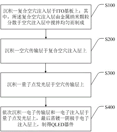
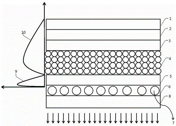
[0029] see figure 1 , figure 1 It is a flow chart of a preferred embodiment of a method for preparing a QLED device with high luminous efficiency in the present invention, as shown in the figure, which includes steps:
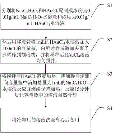
[0030] S100, depositing a composite hole injection layer on the ITO substrate; wherein, the composite hole injection layer is made by dispersing metal nanoparticles in the hole injection layer and stirring uniformly;
[0031] S200, depositing a hole transport layer on the composite hole injection layer;
[0032] S300, deposi...
PUM
| Property | Measurement | Unit |
|---|---|---|
| Thickness | aaaaa | aaaaa |
| Thickness | aaaaa | aaaaa |
| Thickness | aaaaa | aaaaa |
Abstract
Description
Claims
Application Information