Method of making optical planar waveguide

A production method and optical plane technology, applied in the field of optical waveguides, can solve the problems of small batches, the processing technology of optical plane waveguide plates is not very mature, etc., and achieve the effect of reducing half-wave voltage

Inactive Publication Date: 2015-12-16
FUJIAN CASTECH CRYSTALS
View PDF6 Cites 2 Cited by
  • Summary
  • Abstract
  • Description
  • Claims
  • Application Information

AI Technical Summary

Problems solved by technology

[0003] Optical fiber and flat optical waveguide have always been two important dielectric cavities in the field of laser transmission. The manufacturing technology of optical fiber is quite mature, but the processing technology of optical planar waveguide plate is not very mature. Although there are various methods, it can be done very few batches

Method used


Image

  • Method of making optical planar waveguide
  • Method of making optical planar waveguide
  • Method of making optical planar waveguide

Examples


Embodiment Construction

[0012] Below in conjunction with accompanying drawing, patent of the present invention is described further:

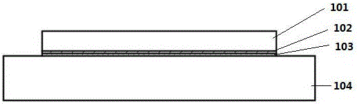
[0013] Such as figure 1 As shown, the side heat dissipation conditions of the waveguide laser microchip are very good, and the heat dissipation of the laser crystal can be greatly improved by bonding without introducing a large stress. For improving the light extraction efficiency of Nd:YVO4, Nd:YAG, Nd:YLF, Yb:YAG and other waveguide lasers. 101 is a laser microchip, 102 and 103 are metal films of the same type (indium film or silver film or gold film), 104 is a substrate, 102 metal film is plated on the side of 101 laser microchip, 103 metal film is plated on 104 substrate . Under the condition of applying uniform pressure between 101 and 104, the two are bonded together by using metal as a bonding medium.

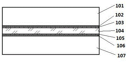
[0014] Such as figure 2 As shown, 101, 107 are substrates; 102, 103, 105, 106 are metal films; 104 is BBO. With this structure, the crystal is calculated ...


PUM


Abstract

The invention discloses a method of making an optical planar waveguide. According to the invention, the cold welding process is used for bonding a laser crystal waveguide strip and an electro-optical crystal waveguide strip, excellent heat dissipation of a device at work can be achieved through accurate pressure control and selection of appropriate bonding material and substrate material, and internal stress accumulation due to uneven pressure can be eliminated. The making method is mature and high in consistency and can be batched.

Description

technical field [0001] The patent of the present invention relates to the field of optical waveguide technology, in particular to a cold pressure welding process for bonding laser crystals and components. Background technique [0002] Different materials have different physical properties, such as mobility, optical absorption properties, thermal conductivity, and mechanical properties. For an application, one material often cannot meet all the required optical properties, so two or more materials need to be integrated. Over the past few decades, people have been exploring ways to integrate different materials to create more powerful and superior devices. [0003] Optical fiber and flat optical waveguide have always been two important dielectric cavities in the field of laser transmission. The manufacturing technology of optical fiber is quite mature, but the processing technology of optical planar waveguide plate is not very mature. Although there are various methods, it ca...

Claims


Application Information

Patent Timeline
Patent Type & Authority Applications(China)
IPC IPC(8): G02B6/12G02B6/00F21V8/00
CPCG02B6/0065G02B6/0033G02B6/12G02B2006/12166
Inventor 校金涛江彬王城强欧阳靖吴季陈伟
Owner FUJIAN CASTECH CRYSTALS
Why Eureka
Try Eureka