Method of manufacturing transverse MOSFET device

A manufacturing method and device technology, applied in semiconductor/solid-state device manufacturing, semiconductor devices, electrical components, etc., can solve problems such as difficulty in obtaining monocrystalline silicon, achieve the effects of avoiding large leakage currents and alleviating conflicting relationships

Inactive Publication Date: 2015-12-16
UNIV OF ELECTRONICS SCI & TECH OF CHINA
View PDF5 Cites 2 Cited by
  • Summary
  • Abstract
  • Description
  • Claims
  • Application Information

AI Technical Summary

Problems solved by technology

At present, silicon-on-insulator can be prepared by bonding, oxygen injection isolation, intelligent stripping and other technologies, but these technologies are used in the material preparation stage, and it is difficult to obtain single crystal silicon on the surface of silicon dioxide in the subsequent process

Method used


Image

  • Method of manufacturing transverse MOSFET device
  • Method of manufacturing transverse MOSFET device
  • Method of manufacturing transverse MOSFET device

Examples


Embodiment 1

[0049] The manufacturing process of the lateral MOSFT device in this example is as follows:

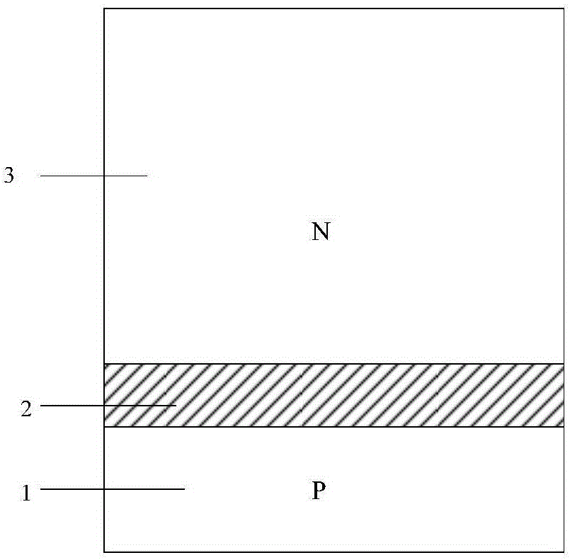
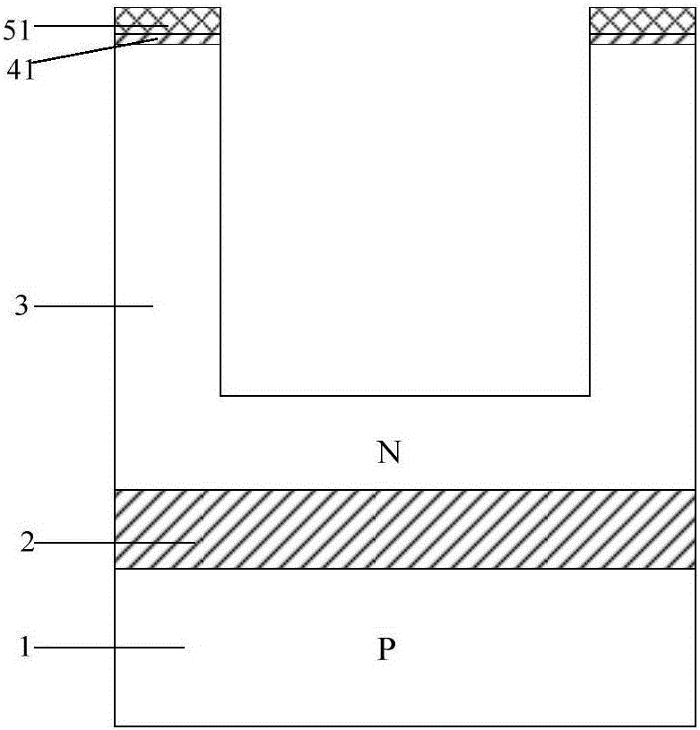
[0050] Preparation materials: SOI materials (such as figure 2 shown) includes a bottom-up substrate layer 1, a dielectric buried layer 2 and an active layer 3, wherein the conductivity type of the substrate layer 1 is not limited, and the conductivity type of the active layer 3 is the first conductivity type:

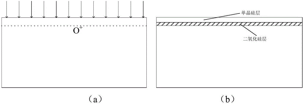
[0051] Step 1: forming a first groove. A thermal oxidation process is used to grow an oxide layer 41 on the surface of the active layer 3, and deposit Si on the surface of the oxide layer 41 3 N 4 Layer 51, according to the photolithography window, sequentially etches Si 3 N 4 layer 51, oxide layer 41 and active layer 3 to a set depth to form a first trench (such as image 3 shown);

[0052] Step 2: forming a dielectric layer inside the active layer, and leaving single crystal silicon inside the dielectric layer. Forming the gate dielectric layer adopts an inclined ion ...

Embodiment 2

[0066] The difference between this example and Example 1 is that the ions implanted in step 2 can be oxygen ions, nitrogen ions, or other ions that can react with the active layer material to form an insulating dielectric layer; the gate dielectric layer obtained by reacting the ions with silicon 6 can be silicon dioxide, silicon nitride or other insulating media.

Embodiment 3

[0068] This example differs from Example 1 in that step 6 is performed by thermal growth or deposition when filling the insulating medium 8 in the second trench; the medium grown by deposition is not as dense as the medium grown by thermal growth, and can be High temperature densification is selected, and in the case of thicker insulating medium in the first trench, multiple depositions are used to fill it.


PUM


Abstract

The invention belongs to the semiconductor technical field and specifically relates to a groove type transverse MOSFET device manufacturing method. The method mainly comprises the following steps of making injected ions and silicon react to form a U type dielectric layer through technical steps of deep groove etching, inclined ion injection, high-temperature annealing, epitaxy, etc.; making a monocrystalline silicon layer reserved on the surface of the dielectric layer; acquiring a monocrystalline silicon semiconductor layer for device manufacturing on the surface of the monocrystalline silicon layer through epitaxial technologies; providing a monocrystalline silicon layer of a device active region and achieving technical manufacturing of the groove type transverse semiconductor device. The method has the following advantages that a monocrystalline silicon material can be acquired on the dielectric layer film; and defects caused by the polysilicon serving as the active region and characterized by large leakage current, low breakdown voltage and bad technical repeatability, etc. can be prevented.

Description

technical field [0001] The present invention belongs to semiconductor technology, specifically relates to MOSFET (MetalOxideSemiconductorfieldeffecttransistor, metal-oxide-semiconductor field effect transistor) device, particularly LDMOS (LateralDouble-diffusionMetalOxideSemiconductorfieldeffecttransistor, lateral double-diffusion metal-oxide-semiconductor fieldeffecttransistor) device Manufacturing method. Background technique [0002] Two key parameters of a power MOSFET are withstand voltage (BV) and specific on-resistance (R on.sp ). The withstand voltage can be improved by increasing the length of the drift region and reducing the doping concentration of the drift region. However, both methods will increase the specific on-resistance of the device. In a conventional power MOSFET, the specific on-resistance R on,sp According to the relationship with the withstand voltage BV R on,sp ∝BV 2.5 This contradictory relationship seriously restricts the development of power ...

Claims


Application Information

Patent Timeline
Patent Type & Authority Applications(China)
IPC IPC(8): H01L21/336H01L29/04
CPCH01L29/04H01L29/66704
Inventor 罗小蓉刘建平张彦辉谭桥尹超周坤魏杰阮新亮李鹏程张波
Owner UNIV OF ELECTRONICS SCI & TECH OF CHINA
Why Eureka
Try Eureka