

Flexible two-dimensional material light emitting device
A technology of light-emitting devices and two-dimensional materials, applied in semiconductor devices, electrical components, circuits, etc., can solve the problems of high cost, difficult process, difficult mass production, etc., and achieve low production cost, easy mass production, and easy batch production. production effect
- Summary
- Abstract
- Description
- Claims
- Application Information
AI Technical Summary
Problems solved by technology
Method used
Image

Examples
Embodiment 1
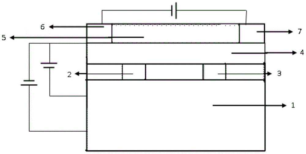
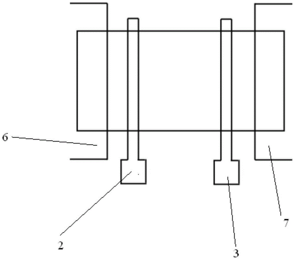
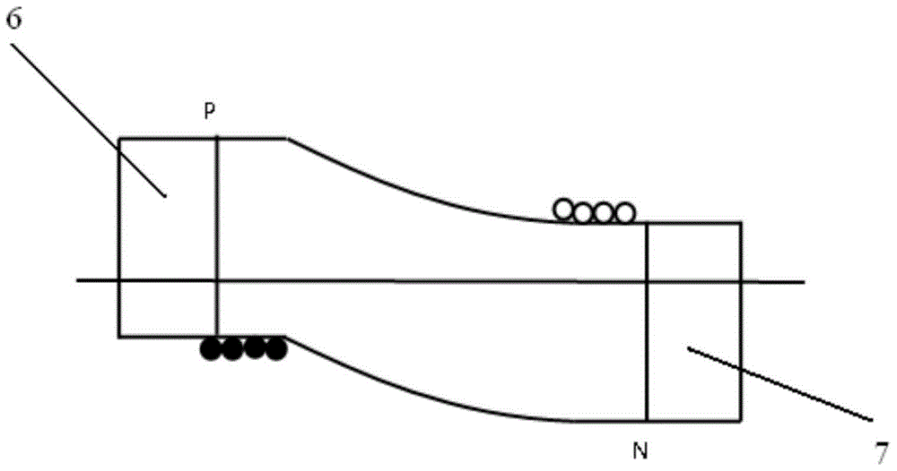
[0034] Such as figure 1 As shown, a flexible two-dimensional material light-emitting device is used to emit red light with a wavelength of 500-700 nm. The light-emitting device includes a flexible substrate layer 1, a first metal layer, a dielectric layer 4, and a two-dimensional semiconductor material from bottom to top Layer 5, and the second metal layer disposed on the dielectric layer 4 and located at both ends of the two-dimensional semiconductor material layer 5, the flexible substrate layer 1 is made of polyethylene terephthalate, and the dielectric layer 4 is made of transparent Al 2 o 3 made, the thickness of the dielectric layer 4 is within 50nm, and the semiconducting material of the two-dimensional semiconductor material layer 5 is MoS 2 , the dielectric layer 4 is used as a gate, and the two ends of the second metal layer are respectively used as a source and a drain, thereby forming a MOS structure;
[0035] The left and right sides of the first metal layer are...
Embodiment 2
[0045] A flexible two-dimensional material light-emitting device for emitting red light with a wavelength of 500-700nm, the light-emitting device sequentially includes a flexible substrate layer, a first metal layer, a dielectric layer, a two-dimensional semiconductor material layer, and a The second metal layer on the dielectric layer and located at both ends of the two-dimensional semiconductor material layer, the flexible substrate layer is made of polyimide, the dielectric layer is made of ferroelectric dielectric, the thickness of the dielectric layer is 50nm, half of the two-dimensional semiconductor material layer conductive material is MoS 2 , the dielectric layer is used as the gate, and the two ends of the second metal layer are respectively used as the source and drain, thus forming a MOS structure;
[0046] The left and right sides of the first metal layer are respectively provided with a first metal electrode and a second metal electrode, the material of the first...
Embodiment 3
[0048] A flexible two-dimensional material light-emitting device for emitting red light with a wavelength of 500-700nm, the light-emitting device sequentially includes a flexible substrate layer, a first metal layer, a dielectric layer, a two-dimensional semiconductor material layer, and a The second metal layer on the dielectric layer and located at both ends of the two-dimensional semiconductor material layer, the flexible substrate layer is made of polyethylene naphthalate, and the dielectric layer is made of organic materials such as polytetravinylphenol, polyvinylpyrrolidone or polymethacrylic acid One of the methyl esters. The thickness of the dielectric layer is 10nm, and the semiconducting material of the two-dimensional semiconductor material layer is MoS 2 , the dielectric layer is used as the gate, and the two ends of the second metal layer are respectively used as the source and drain, thus forming a MOS structure;
[0049] The left and right sides of the first me...
PUM
 Abstract
Description
Claims
Application Information