A bendable and foldable heterogeneous flexible thermoelectric conversion device
A thermoelectric conversion device, a technology of bending and folding, which is applied in the direction of thermoelectric devices that only utilize the Peltier or Seebeck effect, and achieves the effects of high-density integration, simple overall structure, and good application prospects.
- Summary
- Abstract
- Description
- Claims
- Application Information
AI Technical Summary
Problems solved by technology
Method used
Image
Examples
Embodiment 1
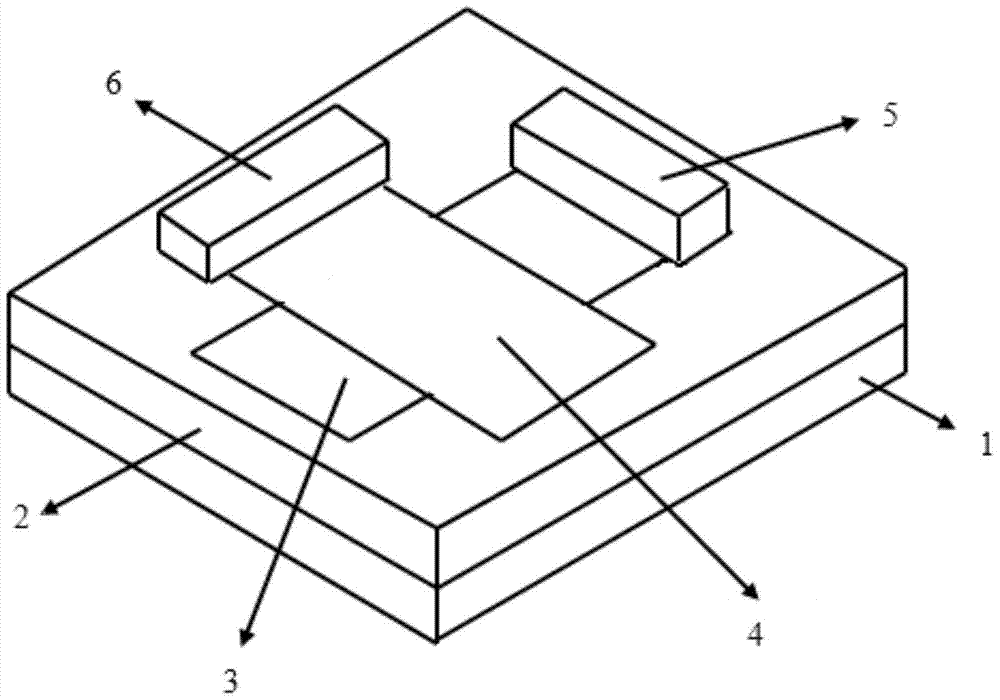
[0031] Such as figure 1 As shown, a bendable and foldable heterogeneous flexible thermoelectric conversion device, the heterogeneous flexible thermoelectric conversion device includes a flexible substrate 1, a dielectric layer 2 sequentially grown on the flexible substrate 1 and a heterostructure, the heterostructure includes The graphene layer 3 and the two-dimensional semiconductor crystal layer 4 overlapped from bottom to top, the first metal electrode 5 is grown on one end of the graphene layer 3, the second metal electrode 6 is grown on one end of the two-dimensional semiconductor crystal layer 4, and the first metal electrode 5 and the second metal electrode 6 are isolated from each other; during operation, under the radiation of an external heat source, a temperature gradient is generated in the overlapping region of the graphene layer 3 and the two-dimensional semiconductor crystal layer 4, which causes the Seebeck effect and generates an open circuit voltage. and perf...
Embodiment 2
[0037] In the present embodiment, the material of the flexible substrate 1 is polyethylene naphthalate, the dielectric layer 2 is a silicon dioxide dielectric layer, and the thickness of the silicon dioxide dielectric layer is 80nm; the thickness of the graphene layer 3 is 15nm , and the thickness of the two-dimensional semiconductor crystal layer 4 is 50nm, and the material of the two-dimensional semiconductor crystal layer 4 is MoSe 2 .
[0038]During preparation, the graphene layer 3 is obtained through a standard mechanical exfoliation process, and then transferred to the silicon dioxide dielectric layer. The graphene in the graphene layer 3 is multi-layer graphene, and then the two-dimensional semiconductor crystal layer is prepared by mechanical exfoliation 4. Transfer to the graphene layer 3 by transfer technology, and finally, deposit a metal diaphragm on one end of the graphene layer 3 and one end of the two-dimensional semiconductor crystal layer 4 by electron beam e...
Embodiment 3
[0041] In this embodiment, the material of the flexible substrate 1 is polyimide, the dielectric layer 2 is a silicon dioxide dielectric layer, and the thickness of the silicon dioxide dielectric layer is 60nm; the thickness of the graphene layer 3 is 16nm, and the two-dimensional The thickness of the semiconductor crystal layer 4 is 32nm, and the material of the two-dimensional semiconductor crystal layer 4 is WS 2 .
[0042] During preparation, the graphene layer 3 is obtained through a standard mechanical exfoliation process, and then transferred to the silicon dioxide dielectric layer. The graphene in the graphene layer 3 is multi-layer graphene. Subsequently, a two-dimensional semiconductor is prepared by chemical liquid phase synthesis. The crystal layer 4 is transferred to the graphene layer 3 by transfer technology, and finally, a metal diaphragm is deposited on one end of the graphene layer 3 and one end of the two-dimensional semiconductor crystal layer 4 respectivel...
PUM
 Abstract
Description
Claims
Application Information
