

Terahertz frequency band local oscillation source based on frequency multiplication link circuit integrated structure
A technology of terahertz and multiplier chain, which is applied in the field of terahertz frequency band local oscillator, can solve the problems of inconvenient use, standing waves, and large volume, and achieve the effects of improving standing wave performance, improving performance, and overcoming reflections
- Summary
- Abstract
- Description
- Claims
- Application Information
AI Technical Summary
Problems solved by technology
Method used
Image

Examples
Embodiment Construction
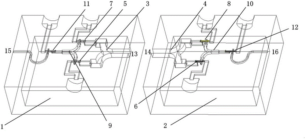
[0024] A terahertz frequency band local oscillator based on the integrated structure of frequency doubling links according to the present invention will be described in detail below with reference to the drawings and embodiments.
[0025] With reference to the terahertz frequency band local oscillator source shown in 1 and 2, the present invention provides a terahertz frequency band local oscillator source based on the integrated structure of frequency doubling links. The local oscillator source includes: an upper cavity 1 and a lower cavity body 2;
[0026] The upper cavity 1 includes: the first Y-junction 3, the first double frequency 5, the third double frequency 7, the third Y-junction 9, the fifth double frequency 11, the first input waveguide port 13 and the first output waveguide port 15;
[0027] The lower cavity 2 includes: the second Y-junction 4, the second double frequency 6, the fourth double frequency 8, the fourth Y-junction 10, the sixth double frequency 12, t...
PUM
 Abstract
Description
Claims
Application Information