Chip-on-film structure and liquid crystal panel provided with same

A soft board and chip technology, which is applied in the field of liquid crystal display, can solve problems such as bad wiring, bonding wires, and lead wires are too thin and secure, and achieve the effects of shortening the lead wire length, increasing the connection area, and stabilizing physical and electrical connections

Inactive Publication Date: 2016-01-20
TCL CHINA STAR OPTOELECTRONICS TECH CO LTD
View PDF7 Cites 14 Cited by
  • Summary
  • Abstract
  • Description
  • Claims
  • Application Information

AI Technical Summary

Problems solved by technology

[0005] The purpose of the present invention is to provide a chip-on-a-flex structure to solve the technical problem of poor bonding in the prior art due to the thin leads and dense wiring of the chip-on-a-flex structure

Method used


Image

  • Chip-on-film structure and liquid crystal panel provided with same
  • Chip-on-film structure and liquid crystal panel provided with same
  • Chip-on-film structure and liquid crystal panel provided with same

Examples


Embodiment Construction

[0021] The following will clearly and completely describe the technical solutions in the embodiments of the present invention with reference to the accompanying drawings in the embodiments of the present invention. Obviously, the described embodiments are only some, not all, embodiments of the present invention. Based on the embodiments of the present invention, all other embodiments obtained by persons of ordinary skill in the art without creative efforts fall within the protection scope of the present invention.

[0022] The invention provides a chip-on-flex structure, which can be applied to electronic devices with display panels, such as mobile phones, tablet computers, notebook computers, liquid crystal displays, liquid crystal televisions, and digital cameras. In this embodiment, the beneficial effects of the present invention are described by taking the liquid crystal panel as an example.

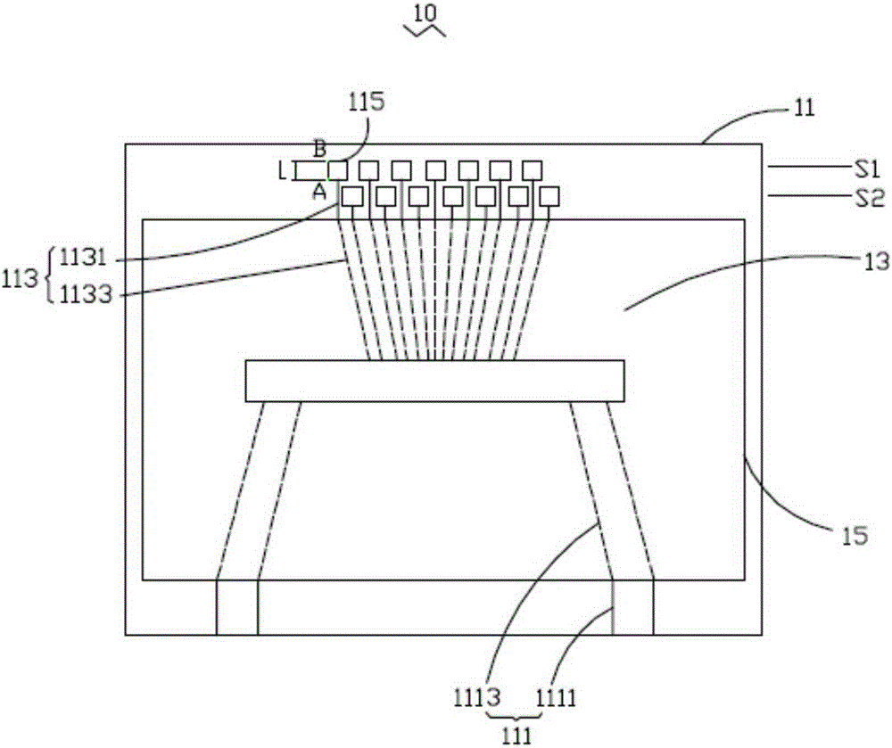
[0023] see figure 1 The chip-on-a-flex structure 10 provided by the first embod...


PUM


Abstract

The invention provides a chip-on-film structure. The structure comprises a film and a driving chip, wherein a set of input end leads and a set of output end leads are arranged on the film, a binding part is formed at the tail end of each output end lead, and the driving chip is arranged on the film and electrically connected to the input end leads and the output end leads. The position, connected with the tail end of the corresponding output end lead, of each binding part is defined as A, the position, away from the tail end of the corresponding output end lead, of each binding part is defined as B, the distance between A and B is L, and the area of each binding part is larger than that of the corresponding output end lead under the length L. According to the chip-on-film structure, binding yield can be increased, and manufacturing cost can be reduced. The invention further provides a liquid crystal panel provided with the chip-on-film structure.

Description

technical field [0001] The invention relates to the technical field of liquid crystal display, in particular to a chip-on-a-flex structure and a liquid crystal panel having the chip-on-a-flex structure. Background technique [0002] There are many types of packaging forms for liquid crystal display (LCD) driver chips, such as quadflatpackage (QFP), chip on glass (chiponglass, COG), tape automated bonding (TAB) and flexible board. Chip (chiponfilm, COF), etc. Among them, the COF flexible chip-on-board structure has become the mainstream of the LCD driver chip packaging process because of its flexibility and the ability to provide smaller pitches. [0003] In the liquid crystal display structure, the source driver chip or the gate driver chip is mounted on the COF. The COF is provided with an input terminal lead (not shown) connected to a printed circuit board (Printed Circuit Board, PCB) and an output terminal lead (not shown) connected to the glass substrate of the liquid ...

Claims


Application Information

Patent Timeline
Patent Type & Authority Applications(China)
IPC IPC(8): G02F1/1345
CPCG02F1/13452G02F1/13458H01L24/48H01L2224/48227H01L2224/49173G02F1/133345H01L2924/1426
Inventor 宋海漫郭东胜
Owner TCL CHINA STAR OPTOELECTRONICS TECH CO LTD
Why Eureka
Try Eureka