Substrate

A substrate and dielectric film technology, which is applied in the plating of superimposed layers, vacuum evaporation plating, coating, etc., can solve the problem of inability to deposit silicon dioxide layers, and achieve the effect of low thermal budget

Active Publication Date: 2016-01-27
SPTS TECH LTD
View PDF4 Cites 0 Cited by
  • Summary
  • Abstract
  • Description
  • Claims
  • Application Information

AI Technical Summary

Problems solved by technology

However, it is currently not possible to deposit such thick, uniform silica layers at temperatures of 280°C or lower.

Method used


Image

  • Substrate
  • Substrate
  • Substrate

Examples


Embodiment Construction

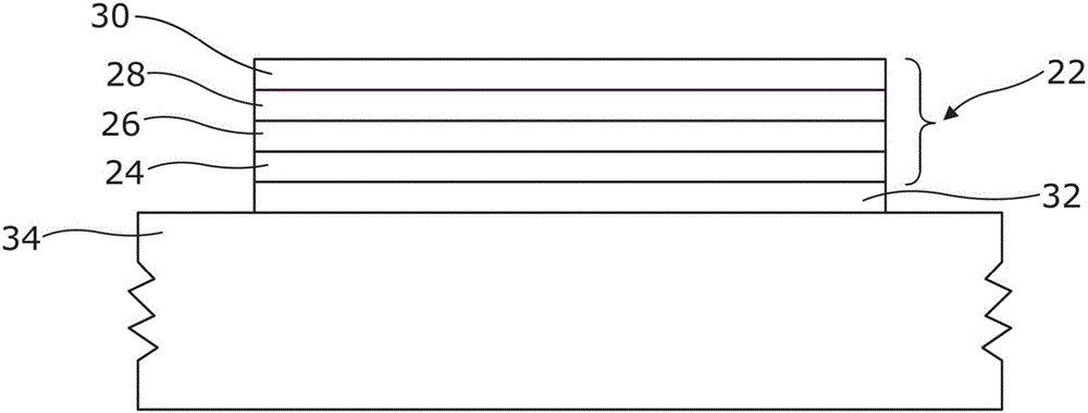
[0047] The present invention provides a dielectric film composed of a plurality of layers. In the film, at least some adjacent layers are subjected to alternating stresses, ie compressive and tensile stresses. By judicious selection of the process parameters used in depositing the dielectric film, any addition of stress to the substrate or structure on which the dielectric film is deposited can be avoided. Alternatively, it is also possible to vary the overall stress experienced by the substrate or structure together with the dielectric film. Typically, the above is done to reduce overall stress.

[0048] The invention is applicable to a wide range of dielectric films that can be deposited on a wide range of substrates. The substrate on which the dielectric film can be deposited may form part of a larger structure. Again, the invention can be used in a wide variety of configurations. An advantage of the present invention is that relatively thick dielectric films can be dep...


PUM

PropertyMeasurementUnit
thicknessaaaaaaaaaa
thicknessaaaaaaaaaa
thicknessaaaaaaaaaa

Abstract

A substrate having a dielectric film thereon, in which: the dielectric film comprises at least four stacked layers of a dielectric material; the stacked layers comprise compressive layers which are subject to a compressive stress, and tensile layers which are subject to a tensile stress; and there are at least two spaced apart tensile layers which are each adjacent to one or more compressive layers.

Description

technical field [0001] The present invention relates to a substrate having a dielectric film thereon, a method of depositing a dielectric film on the substrate and related apparatus. Background technique [0002] Many devices are fabricated by building up multiple thin dielectric, semiconducting, and metal layers on a substrate such as a silicon wafer. However, the deposition of these layers results in a build-up of stress. The net stress generated at each stage leads to constraints in subsequent processing steps. For example, the resulting net stress can lead to warping of the wafer, which can eventually lead to wafer loss due to handling issues. A further problem is layer cracking, which in turn leads to reduced yield and wafer loss. The net stress experienced by the wafer may be tensile or compressive. [0003] It is standard practice in semiconductor wafer fabrication to minimize wafer warpage. Another standard practice is to deposit layers without creating cracks a...

Claims


Application Information

Patent Timeline
Patent Type & Authority Applications(China)
IPC IPC(8): H01L23/14H01L21/316
CPCH01L23/3192H01L23/562H01L2924/0002C23C16/401C23C16/45523C23C28/04H01L28/40H01L2924/00H01L21/02118H01L21/02164H01L21/02274H01L21/02214C23C14/10
Inventor 凯瑟琳·克鲁克斯蒂芬·R·伯吉斯
Owner SPTS TECH LTD
Why Eureka
Try Eureka