A MOS resistor and its manufacture method

A technology of MOS transistors and manufacturing methods, which is applied in the field of MOS transistors with new structures and their manufacturing, can solve the problems of reducing the on-state current of devices, high thermal budget, and difficulty in application, and achieve the reduction of off-state leakage current and switch-state current The effect of improving and lowering the thermal budget

Inactive Publication Date: 2007-05-16
PEKING UNIV
View PDF0 Cites 7 Cited by
  • Summary
  • Abstract
  • Description
  • Claims
  • Application Information

AI Technical Summary

Problems solved by technology

Some researchers have proposed a Schottky barrier source-drain MOSFET with source-drain elevation, that is, a recessed gate. This structure device has a large on-off current ratio, but its source terminal is raised while reducing the device On-state current, and at the same time, there are difficulties in the realization of the device process at the nanometer scale
Some researchers have also proposed that the source end uses metal or metal silicide to form a Schottky barrier, and the drain end uses doping implantation to form a PN junction. This device structure has good device characteristics, but self-alignment cannot be achieved in the process. Simultaneous doping Implantation is done after the gate structure is formed, which means a high thermal budget, making it difficult to apply to nanoscale MOSFET fabrication

Method used


Image

  • A MOS resistor and its manufacture method
  • A MOS resistor and its manufacture method
  • A MOS resistor and its manufacture method

Examples


Embodiment Construction

[0039] The following specific examples help to understand the characteristics and advantages of the present invention, but the implementation of the present invention is by no means limited to the described examples.

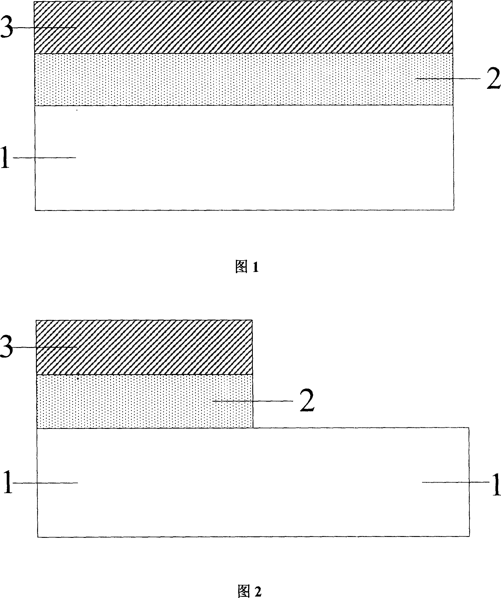
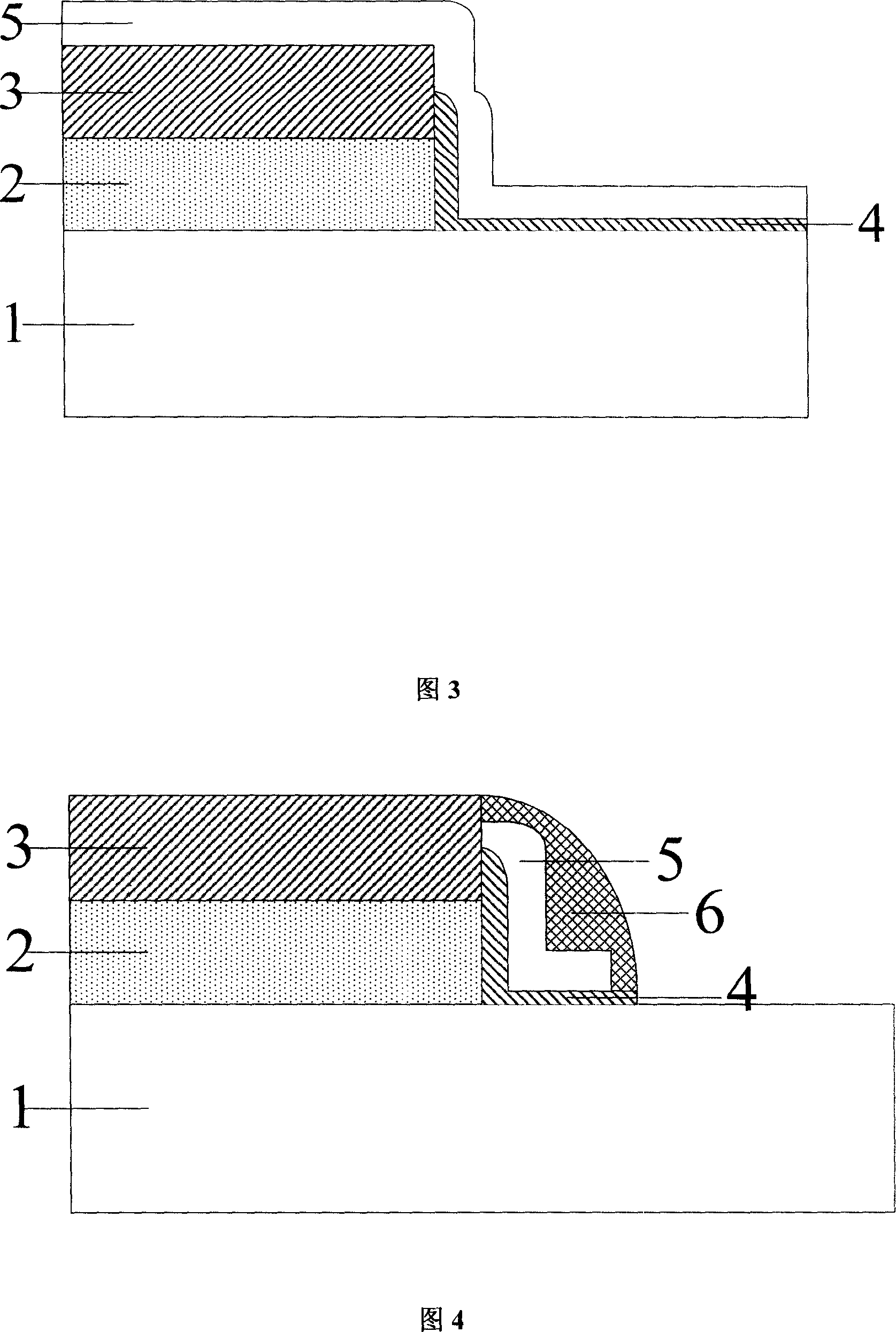
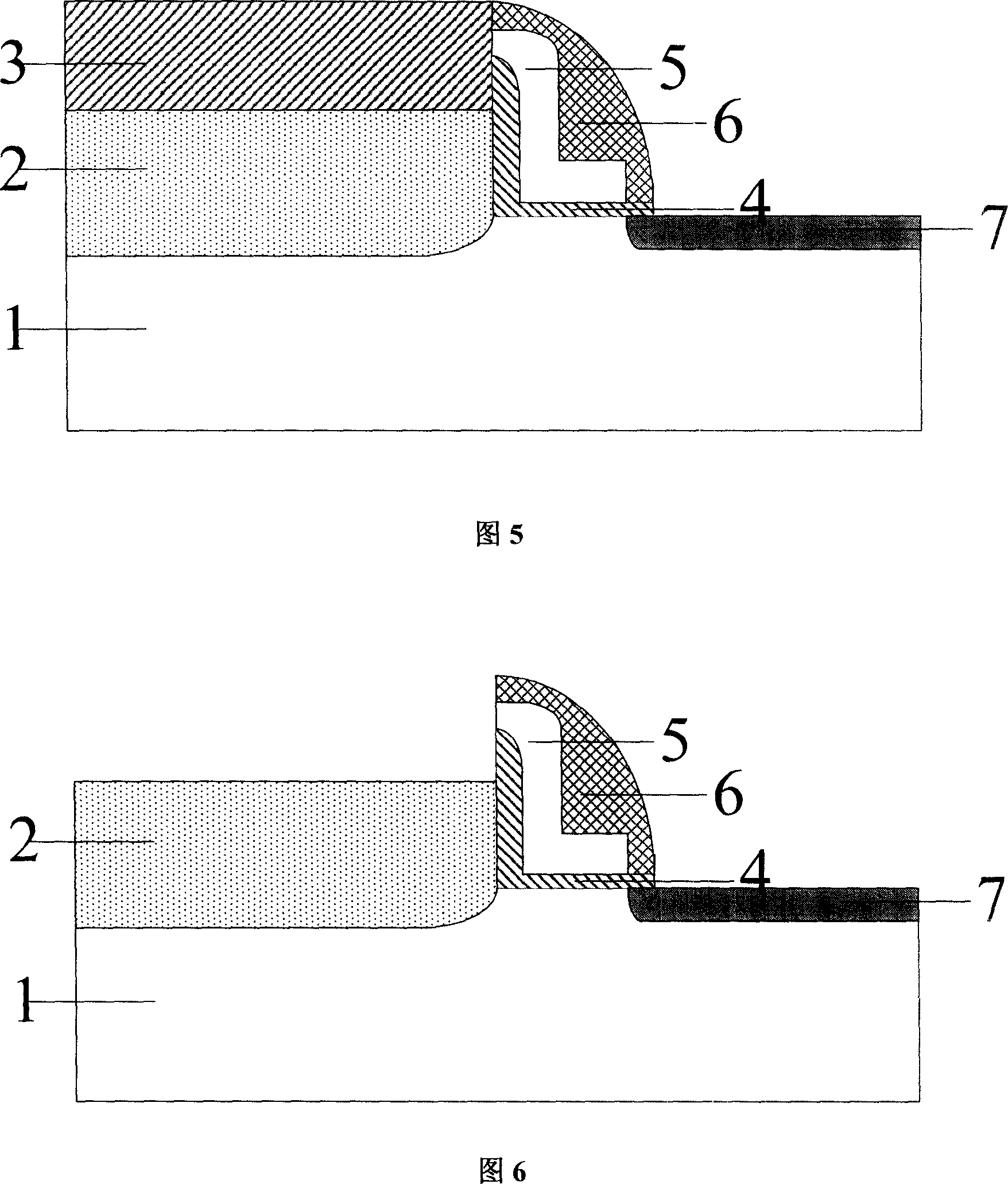
[0040] A specific embodiment of the manufacturing method of the present invention comprises the process steps shown in Fig. 1 to Fig. 6:

[0041] 1. As shown in Figure 1, the crystal orientation of the bulk silicon substrate (1) used is (100), the body region is initially lightly doped, and the active region is fabricated on the substrate using conventional CMOS shallow trench isolation technology Isolation layer; then perform ion implantation, the ion implantation energy is 30KeV, and the implanted impurity is As; then deposit a layer of TEOS dielectric protection layer (2) with a thickness of 50-100nm.

[0042] 2. As shown in FIG. 2, perform photolithography once, etch the TEOS dielectric protection layer (3), and then etch the doped silicon layer (2) until th...


PUM


Abstract

The provided MOS transistor comprises asymmetric source and drain structures. Wherein, the source uses metal or metal-semiconductor compound and channel to form Schottky barrier contact, while the drain is boost high doped. Compared with traditional MOSFET device, this invention increases on-off current rate greatly, compatible to traditional manufacture technology, and has much room for high-K grid medium and metal grid material since low thermal budget.

Description

Technical field: [0001] The invention belongs to the technical field of semiconductor integrated circuits and its manufacture, and in particular relates to a MOS transistor with a new structure and a manufacturing method thereof. Background technique: [0002] In the contemporary information society, driven by the dual drive of chip integration density maximization and circuit performance optimization, the core MOSFET devices of integrated circuits are continuously scaled down. With the continuous shrinking of the size of MOSFET devices, when the feature size of devices enters the nanometer scale, integrated circuits with MOSFETs as the core encounter more and more challenges in many fields such as materials, structures and processes. In order to meet these challenges, many new device structures and process fabrication methods have been proposed and applied to the design and manufacture of nanometer-scale MOSFETs. [0003] Schottky barrier source-drain MOSFET is one of them...

Claims


Application Information

Patent Timeline
Patent Type & Authority Applications(China)
IPC IPC(8): H01L29/78H01L21/336
Inventor 孙雷李定宇张盛东吴涛韩汝琦刘晓彦
Owner PEKING UNIV
Why Eureka
Try Eureka