Semiconductor device and forming method thereof

A semiconductor and device technology, applied in the field of semiconductor devices and their formation, can solve problems such as unstable threshold voltage adjustment, and achieve the effect of good shape and stable performance

Active Publication Date: 2016-02-03
SEMICON MFG INT (SHANGHAI) CORP
View PDF3 Cites 21 Cited by
  • Summary
  • Abstract
  • Description
  • Claims
  • Application Information

AI Technical Summary

Problems solved by technology

[0005] However, in the formed CMOS transistor with a work funct

Method used


Image

  • Semiconductor device and forming method thereof
  • Semiconductor device and forming method thereof
  • Semiconductor device and forming method thereof

Examples


Embodiment Construction

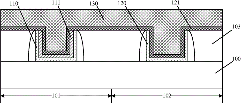
[0033] As mentioned in the background, in the CMOS transistors with work function layers formed in the prior art, the adjustment of the threshold voltage is unstable.

[0034] After research, please refer to figure 1 , figure 1 It is a schematic cross-sectional structure diagram of a process of forming a complementary metal oxide semiconductor transistor embodiment, including: providing a substrate 100, the substrate 100 has an NMOS region 102 and a PMOS region 101; the surface of the substrate 100 has a dielectric layer 103 There is a first opening (not shown) exposing the surface of the substrate 100 in the dielectric layer 103 of the PMOS region 101, and there is a second opening (not shown) exposing the substrate 100 surface in the dielectric layer 103 of the NMOS region 102 not shown), the sidewall and bottom surface of the first opening have a first gate dielectric layer 110, the sidewall and bottom surface of the second opening have a second gate dielectric layer 120, ...


PUM

PropertyMeasurementUnit
Thicknessaaaaaaaaaa
Thicknessaaaaaaaaaa

Abstract

The invention discloses a semiconductor device and a forming method thereof. The forming method of the semiconductor device comprises the steps as follows: a substrate including a first region and a second region is provided; a dielectric layer is arranged on the surface of the substrate; a first opening for exposing the surface of the substrate is formed in the dielectric layer of the first region; a second opening for exposing the surface of the substrate is formed in the dielectric layer of the second region; a first gate dielectric layer is arranged at the bottom of the first opening; a second gate dielectric layer is arranged at the bottom of the second opening; a first work function layer is formed on the side wall and the bottom surface of the first opening; a work function barrier layer is formed on the surface of the first work function layer; a second work function layer is formed on the dielectric layer, the work function barrier layer, and the side wall and the bottom surface of the second opening; the work function barrier layer is used for blocking mutual diffusion of materials of the first work function layer and the second work function layer; after the second work function layer is formed, a first gate electrode layer for fully filling the first opening and a second gate electrode layer for fully filling the second opening are formed; and the performance of the formed semiconductor is improved.

Description

technical field [0001] The invention relates to the technical field of semiconductor manufacturing, in particular to a semiconductor device and a forming method thereof. Background technique [0002] Complementary Metal-Oxide-Semiconductor (CMOS) is one of the basic semiconductor devices that constitute integrated circuits. The complementary metal oxide semiconductor transistor includes: P-type metal oxide semiconductor (PMOS) and N-type metal oxide semiconductor (NMOS). [0003] In the prior art, in order to control the short channel effect while reducing the gate size, high-K dielectric materials are used instead of conventional silicon oxide and other materials as the gate dielectric layer of transistors, and metal materials are used instead of conventional polysilicon and other materials as the gate dielectric layer of transistors. electrode layer. Moreover, in order to adjust the threshold voltage of the PMOS tube and the NMOS tube, the prior art will form a work func...

Claims


Application Information

Patent Timeline
IPC IPC(8): H01L21/8238H01L27/02
Inventor 徐建华
Owner SEMICON MFG INT (SHANGHAI) CORP
Why Eureka
Try Eureka