Method for regulating and controlling spin orbit coupling of semiconductor quantum well of sphalerite structure

A spin-orbit coupling and semiconductor technology, applied in semiconductor devices, electrical components, circuits, etc., can solve problems such as difficult operation and complex structure, and achieve the effect of simple structure design, easy operation, and obvious control effect

Inactive Publication Date: 2016-02-03
FUZHOU UNIV
View PDF3 Cites 7 Cited by
  • Summary
  • Abstract
  • Description
  • Claims
  • Application Information

AI Technical Summary

Problems solved by technology

However, these two methods are relatively complex in structure, and the last method needs to introduce a variable temperature system, which is difficult to operate

Method used


Image

  • Method for regulating and controlling spin orbit coupling of semiconductor quantum well of sphalerite structure
  • Method for regulating and controlling spin orbit coupling of semiconductor quantum well of sphalerite structure
  • Method for regulating and controlling spin orbit coupling of semiconductor quantum well of sphalerite structure

Examples


Embodiment Construction

[0045] The present invention will be further described below in conjunction with the accompanying drawings and embodiments.

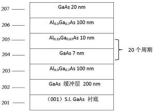
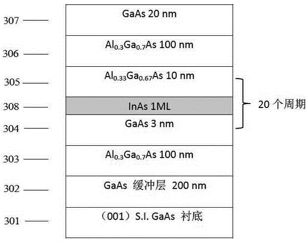
[0046] This embodiment provides a method for regulating the spin-orbit coupling of a semiconductor quantum well with a sphalerite structure, which specifically includes the following steps:

[0047] Step S1: selecting qualified semiconductor quantum well materials;

[0048] Step S2: using molecular beam epitaxy equipment to grow semiconductor quantum wells with different well widths;

[0049] Step S3: measuring the Rashba and Dresselhaus spin-orbit coupling ratios of the semiconductor quantum wells in step S2.

[0050] In this embodiment, the conditions described in step S1 are: the semiconductor quantum well material is a zinc blende structure, the semiconductor quantum well material is a single crystal, and the well width of the semiconductor quantum well material is several nanometers to tens of nanometers.

[0051] In this embodiment, in the step...


PUM


Abstract

The invention relates to a method for regulating and controlling the spin orbit coupling of a semiconductor quantum well of a sphalerite structure. The spin orbit coupling proportion of Rashba to Dresselhaus of the semiconductor quantum well is regulated and controlled by changing the width of the semiconductor quantum well of the sphalerite structure and inserting an ultrathin InAs layer to one interface of the quantum well. The method is easy, and the regulation and control effect is obvious.

Description

technical field [0001] The invention relates to the field of semiconductor spin electronics, in particular to a method for regulating the spin-orbit coupling of a semiconductor quantum well with a sphalerite structure. Background technique [0002] Electrons have two properties, one is spin property and the other is charge property. Since the energy required to manipulate electron spin is much smaller than that of charge, spintronics, which uses spin as an information carrier, has attracted widespread attention. One branch of spintronics is semiconductor spintronics, which regulates the spin state of electrons through the equivalent magnetic field generated by spin-orbit coupling. Because it can be better compatible with the traditional semiconductor process and does not need to apply an external magnetic field, it has a good application prospect. In the study of semiconductor spintronics, spin-orbit coupling has become a current research hotspot. There are two different ...

Claims


Application Information

Patent Timeline
Patent Type & Authority Applications(China)
IPC IPC(8): H01L29/15H01L29/66
CPCH01L29/151H01L29/66984
Inventor 俞金玲陈涌海程树英赖云锋郑巧
Owner FUZHOU UNIV
Why Eureka
Try Eureka