
Method for preparing interface layer of high-k dielectric layer

A technology of dielectric layer and interface layer, applied in semiconductor/solid-state device manufacturing, electrical components, circuits, etc., can solve problems such as difficulty in reducing the equivalent thickness of oxides

Active Publication Date: 2018-07-20
SHANGHAI HUALI MICROELECTRONICS CORP
View PDF3 Cites 0 Cited by
  • Summary
  • Abstract
  • Description
  • Claims
  • Application Information

AI Technical Summary

Problems solved by technology

[0009] Since the high-K gate dielectric material is mainly metal oxide, there must be oxygen in the preparation process, and the reaction between oxygen and silicon will form silicon dioxide or silicide between the high-K dielectric layer and the silicon substrate. Interface oxide layer, due to the existence of the oxide layer, the reduction of the equivalent oxide thickness (EOT) becomes difficult

Method used


Image

  • Method for preparing interface layer of high-k dielectric layer

Examples


Embodiment Construction

[0031] In order to make the content of the present invention clearer and easier to understand, the content of the present invention will be described in detail below in conjunction with specific embodiments and accompanying drawings.

[0032] In the present invention, the combination of in-situ water vapor generation ISSG and flash lamp annealing (Flash Anneal) or rapid thermal oxidation and flash lamp annealing is used for interfacial layer growth to prepare ultra-thin SiO 2 or SiON layer. The interface layer prepared by this method is denser, which can effectively suppress the interface oxide layer formed by subsequent high-K dielectric layer deposition and high-K post-annealing.

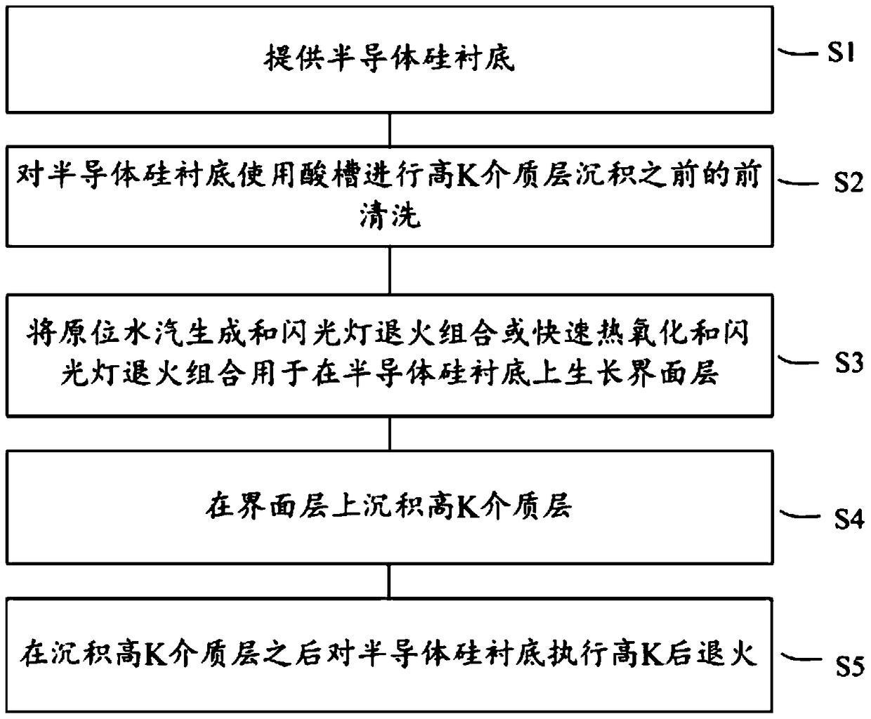
[0033] figure 1 A flow chart of a method for preparing an interface layer of a high-K dielectric layer according to a preferred embodiment of the present invention is schematically shown.

[0034] Such as figure 1 As shown, the method for preparing the interface layer of the high-K dielectric l...


PUM


Abstract

The invention provides a method for preparing the interface layer of a high-K dielectric layer. The method includes the following steps that: first step, a semiconductor silicon substrate is provided; second step, pre-cleaning before high-K dielectric layer deposition is performed on the semiconductor silicon substrate through using an acid tank; third step, in situ steam generation and flash lamp annealing combination or rapid thermal oxidation and flash lamp annealing combination is applied to the growth of the interface layer on the semiconductor silicon substrate; fourth step, the high-K dielectric layer is deposited on the interface layer; and fifth step, after the deposition of the high-k dielectric layer, post high-K annealing is performed on the semiconductor silicon substrate.

Description

technical field [0001] The invention relates to the field of semiconductor manufacturing, more specifically, the invention relates to a method for preparing an interface layer of a high-K (high dielectric constant) dielectric layer. Background technique [0002] With the rapid development of Very Large Scale Integration (VLSI) and Ultra Large Scale Integration (ULSI), the size of MOS devices has been continuously reduced. In order to increase the response speed of the device, increase the driving current and the capacity of the storage capacitor, the thickness of the gate oxide layer in the device is continuously reduced. However, two subsequent problems have become important factors hindering the further development of integrated circuits: leakage and breakdown. When the gate oxide thickness is less than Due to the quantum tunneling effect, carriers can flow through this ultra-thin gate dielectric, and the probability of carrier tunneling increases exponentially with the...

Claims


Application Information

Patent Timeline
Patent Type & Authority Patents(China)
IPC IPC(8): H01L29/423H01L21/02
CPCH01L21/02301H01L21/0231H01L21/02337H01L29/42364
Inventor 肖天金邱裕明温振平
Owner SHANGHAI HUALI MICROELECTRONICS CORP
Learn More