
Patsnap Eureka
For R&D, Patsnap Eureka makes reading and utilizing patents & technical documents easy.
Patsnap Eureka AIR
Designed for self-driven R&D workflows. Generate viable solutions, solve complex R&D challenges, empower your innovation with AI.

Patsnap Eureka Materials
Designed for material experts only. Revolutionize your material R&D, from search, analyze, to developing new materials.

TechResearch
Generate reliable direction feasibility study reports for your R&D in just a few steps.

TechSeek
Discover and master advanced knowledge NOW. Basics, ideas, possibilities, all at once.

TechMind
As an expert in R&D Theories, TechMind can generates customized viable solutions instantly.

TechRisk
Analyze your overall solution with one click, know your potential R&D risks in advance.

TechMonitor
Get weekly tech updates, stay abreast of the latest tech innovations and key insights.
Image processing methods for image sensors with phase detection pixels
A phase detection and pixel technology, applied in the field of imaging system, can solve problems such as difficult correction, and achieve the effect of reducing deviation
- Summary
- Abstract
- Description
- Claims
- Application Information
AI Technical Summary
Problems solved by technology
Method used
Image

Examples
Embodiment Construction
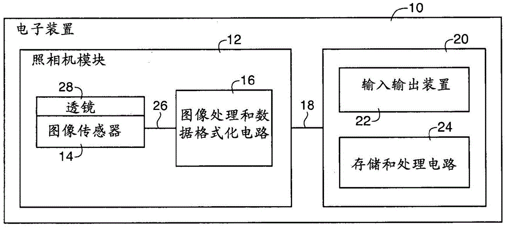
[0029] Embodiments of the invention relate to image sensors with autofocus and depth sensing capabilities. An electronic device with a camera module is shown in figure 1 middle. Electronic device 10 may be a digital camera, computer, cellular phone, medical device, or other electronic device. Camera module 12 (sometimes referred to as an imaging device) may include one or more image sensors 14 and one or more lenses 28 . During operation, lens 28 (sometimes referred to as optics 28 ) focuses light on image sensor 14 . Image sensor 14 includes photosensitive elements (eg, pixels) that convert light into digital data. An image sensor can have any number of pixels (eg, hundreds, thousands, millions, or more). A typical image sensor may, for example, have millions of pixels (eg, megapixels). As examples, image sensor 14 may include bias circuitry (e.g., source follower load circuitry), sample and hold circuitry, correlated double sampling (CDS) circuitry, amplifier circuitry,...
PUM
 Abstract
Description
Claims
Application Information
 - R&D Engineer
- R&D Manager
- IP Professional
- Industry Leading Data Capabilities
- Powerful AI technology
- Patent DNA Extraction
Browse by: Latest US Patents, China's latest patents, Technical Efficacy Thesaurus, Application Domain, Technology Topic, Popular Technical Reports.
© 2024 PatSnap. All rights reserved.Legal|Privacy policy|Modern Slavery Act Transparency Statement|Sitemap|About US| Contact US: help@patsnap.com