Band-gap reference source with low offset voltage and high PSRR (power supply rejection ratio)

A technology of offset voltage and reference source, applied in the direction of adjusting electrical variables, control/regulating systems, instruments, etc., can solve the problem of low output voltage accuracy

Active Publication Date: 2016-02-10
STATE GRID CORP OF CHINA +1
View PDF7 Cites 16 Cited by
  • Summary
  • Abstract
  • Description
  • Claims
  • Application Information

AI Technical Summary

Problems solved by technology

[0011] The purpose of the present invention is to overcome the defect that the bandgap reference source in the prior art is affected by the channel length modulation effect and the output voltage accuracy is not high. According to one aspect of the present invention, a low power consumption and high PSRR bandgap reference source is proposed

Method used


Image

  • Band-gap reference source with low offset voltage and high PSRR (power supply rejection ratio)
  • Band-gap reference source with low offset voltage and high PSRR (power supply rejection ratio)
  • Band-gap reference source with low offset voltage and high PSRR (power supply rejection ratio)

Examples


Embodiment 1

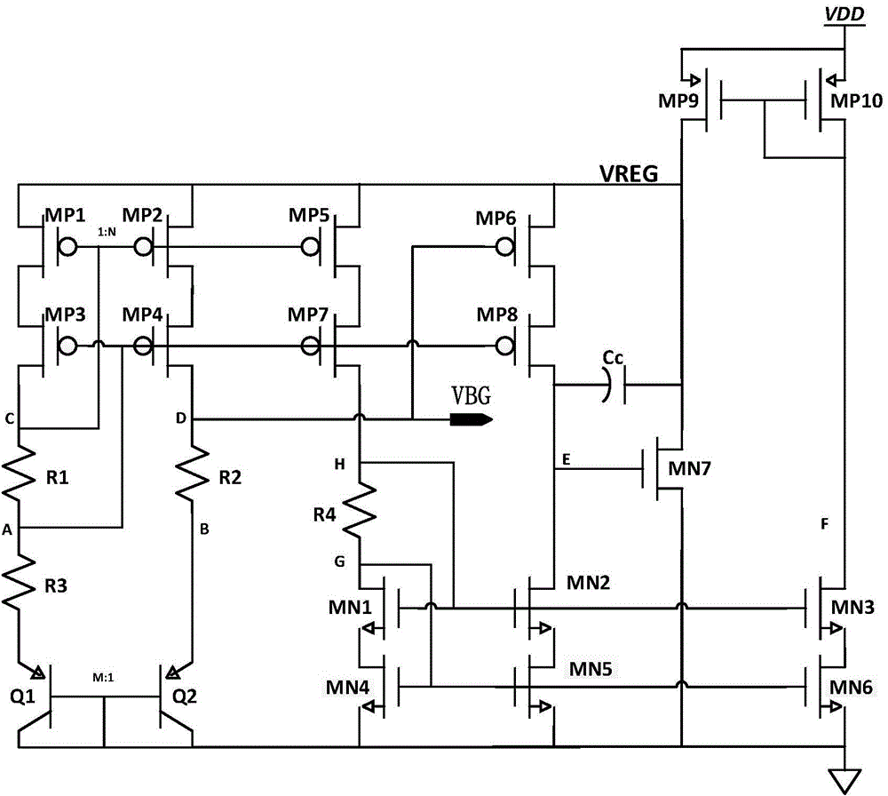
[0090] see image 3 As shown, in the first embodiment, the voltage feedback circuit includes: the fifth P-channel field effect transistor MP5, the sixth P-channel field effect transistor MP6, the seventh P-channel field effect transistor MP7, the eighth P-channel field effect transistor MP8, The ninth P-channel FET MP9, the tenth P-channel FET MP10, the first N-channel FET MN1, the second N-channel FET MN2, the third N-channel FET MN3, and the fourth N-channel FET The effect transistor MN4, the fifth N-channel FET MN5, the sixth N-channel FET MN6, the seventh N-channel FET MN7, the fourth resistor R4, and the compensation capacitor Cc.

[0091] Specifically, see image 3 As shown, the source of the ninth P-channel field effect transistor MP9 is connected to the source of the tenth P-channel field effect transistor MP10 and connected to an external power supply, and the gate of the ninth P-channel field effect transistor MP9 is connected to the tenth P-channel field effect tra...

Embodiment 2

[0110] In Example 2, see Figure 4 As shown, the voltage feedback circuit includes: the fifth P-channel field effect transistor MP5, the sixth P-channel field effect transistor MP6, the seventh P-channel field effect transistor MP7, the eighth P-channel field effect transistor MP8, the ninth P-channel field effect transistor Tube MP9, the tenth P-channel FET MP10, the eleventh P-channel FET MP11, the twelfth P-channel FET MP12, the first N-channel FET MN1, the second N-channel FET MN2, The third N-channel MOSFET MN3, the fourth N-channel MOSFET MN4, the fifth N-channel MOSFET MN5, the sixth N-channel MOSFET MN6, and the compensation capacitor Cc.

[0111] The source of the eleventh P-channel field effect transistor MP11 is connected to the source of the twelfth P-channel field effect transistor MP12 and connected to an external power supply, and the gate of the eleventh P-channel field effect transistor MP11 is connected to the source of the twelfth P-channel field effect tran...


PUM


Abstract

The invention discloses a band-gap reference source with low offset voltage and a high PSRR (power supply rejection ratio). The band-gap reference source comprises a first P-channel field-effect transistor, a second P-channel field-effect transistor, a third P-channel field-effect transistor, a fourth P-channel field-effect transistor, a first resistor, a second resistor, a third resistor, a first bipolar transistor, a second bipolar transistor and a voltage feedback circuit. According to the band-gap reference source with the low offset voltage and the high PSRR, with the adoption of a double-layer current mirror structure and addition of biasing resistors, influence of channel length modulation effects of current mirrors is reduced, the accuracy of current multiplication coefficients is guaranteed, and maladjustment of output voltage is reduced.

Description

technical field [0001] The invention relates to the technical field of bandgap reference sources, in particular to a bandgap reference source with low offset voltage and high PSRR. Background technique [0002] In integrated circuit design, it is mainly divided into two parts: analog circuit and digital circuit. The on-chip bandgap voltage reference source is the core module of the analog circuit, and its performance determines the performance and function realization of the entire analog circuit and even the entire chip. Currently the most widely used bandgap voltage references with the best performance indicators are implemented with bipolar devices. Its principle is to superimpose the voltage with positive temperature coefficient and the voltage with negative temperature coefficient with a certain coefficient to obtain a bandgap voltage with approximately zero temperature coefficient. [0003] With the advancement of technology and the improvement of people's requiremen...

Claims


Application Information

Patent Timeline
Patent Type & Authority Applications(China)
IPC IPC(8): G05F3/26
CPCG05F3/26
Inventor 苏胜新杜新纲杨小坤原义栋胡毅何洋李振国
Owner STATE GRID CORP OF CHINA
Why Eureka
Try Eureka