High-temperature hot stamping film for manufacturing conductive wires, manufacturing method and application for high temperature hot stamping film
A technology of conductive circuit and manufacturing method, which is applied in the direction of transfer printing, conductive pattern formation, photolithography/patterning, etc., can solve the problems of inability to obtain metal coating, film stretching deformation, etc., and achieve the effect of simple structure and low cost
- Summary
- Abstract
- Description
- Claims
- Application Information
AI Technical Summary
Problems solved by technology
Method used
Image
Examples
Embodiment 1
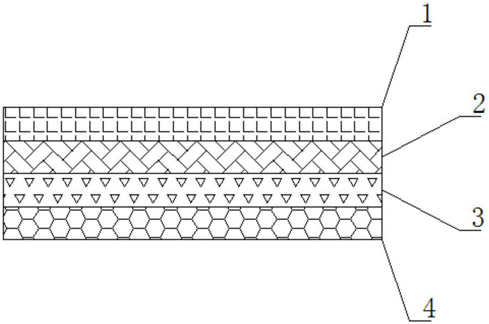
[0034] Coating silicone oil separation layer 1.5g / m2 on 25 micron PET 2 , The measured peeling value is 19.2g / inch. Aluminum is evaporated on a vacuum aluminum plating machine. ×10 -5 Torr's High Vacuum Metallized Aluminum. The conductive square resistance of the conductive layer was measured to be 42 milliohms, and the hot melt adhesive was coated with 1.5g / m 2 , The fixed peeling value of hot stamping film is 3.4g / inch. For a line with a width of 1.6mm hot stamped on coated paper, the burr is 0.08mm.
Embodiment 2
[0036] Coating water-wax separation layer 3g / m on 20 micron PEN 2 , The measured peeling value was 15.2g / inch. Copper was evaporated on a vacuum aluminum plating machine. ×10 -5 Copper metallization under Torr's high vacuum. The conductive square resistance of the conductive layer was measured to be 35 milliohms, and the hot melt adhesive was coated with 2.8g / m 2 , the fixed peeling value is 3.4g / inch. The line burr with a width of 1.0mm on the hot stamping of the PCB is 0.12mm.
Embodiment 3
[0038] Coating water-wax separation layer 2.5g / m on 22 micron PEN 2 , The peeling value was measured to be 17.5g / inch. Copper was evaporated on a vacuum aluminum plating machine. ×10 -5 Copper metallization under Torr's high vacuum. The conductive square resistance of the conductive layer was measured to be 35 milliohms, and the hot melt adhesive was coated with 2.8g / m 2 , the fixed peeling value is 3.4g / inch. The line burr with a width of 1.0mm on the hot stamping of the PCB is 0.12mm.
PUM
| Property | Measurement | Unit |
|---|---|---|
| Withstand temperature | aaaaa | aaaaa |
| Thickness | aaaaa | aaaaa |
| Thickness | aaaaa | aaaaa |
Abstract
Description
Claims
Application Information
