Radiation hardened static random access memory
A technology of static random access and anti-radiation hardening, which is applied in the direction of static memory, digital memory information, information storage, etc., can solve the problems of poor reliability and sensitivity to radiation particles, achieve improved reliability, small impact on circuit system performance, and eliminate effect of influence
- Summary
- Abstract
- Description
- Claims
- Application Information
AI Technical Summary
Problems solved by technology
Method used
Image
Examples
specific Embodiment approach 1
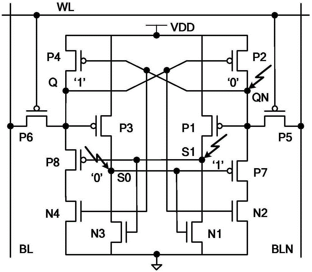
[0021] Specific implementation mode one: refer to figure 1 Describe this embodiment in detail. The anti-radiation hardened static random access memory described in this embodiment includes a No. 1 PMOS transistor P1, a No. 2 PMOS transistor P2, a No. 3 PMOS transistor P3, and a No. 4 PMOS transistor P4. Take the transistor, No. 7 PMOS transistor P7, No. 8 PMOS transistor P8, No. 1 NMOS transistor N1, No. 2 NMOS transistor N2, No. 3 NMOS transistor N3, No. 4 NMOS transistor N4, No. 1 bit line BLN, No. 2 bit line BL and word line WL,
[0022] The access transistors include the fifth PMOS transistor P5 and the sixth PMOS transistor P6,
[0023] The drain of the sixth PMOS transistor P6 is connected to the second bit line BL, and the source of the sixth PMOS transistor P6 is simultaneously connected to the drain of the fourth PMOS transistor P4, the gate of the second PMOS transistor P2, and the gate of the second NMOS transistor N2 The gate of the third PMOS transistor P3 and t...
specific Embodiment approach 2
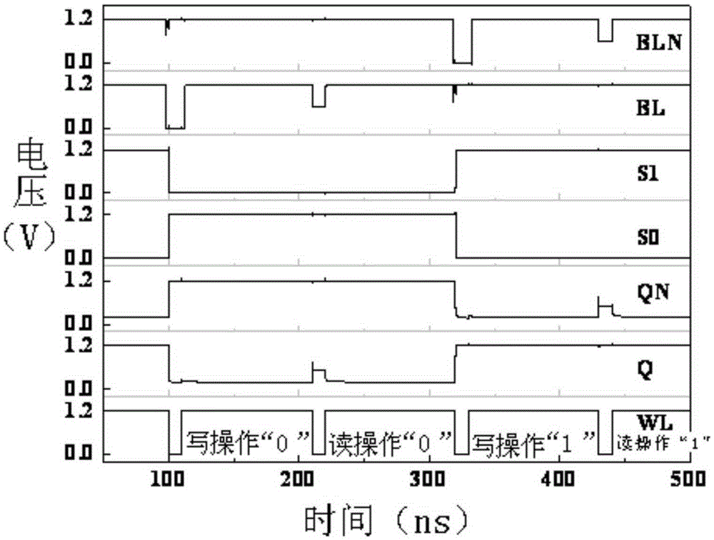
[0045] Embodiment 2: This embodiment is a further description of the anti-radiation hardened SRAM described in Embodiment 1. In this embodiment, when the SRAM is in the storage operation state, the When the line WL is at a high level, the seventh PMOS transistor P7, the fourth PMOS transistor P4, the first PMOS transistor P1, the second NMOS transistor N2 and the third NMOS transistor N3 are all in the on state, and the second PMOS transistor P2 and the third PMOS transistor The transistor P3, the fifth PMOS transistor P5 and the sixth PMOS transistor P6, the first NMOS transistor N1 and the fourth NMOS transistor N4 are all in an off state.
specific Embodiment approach 3
[0046] Specific embodiment three: This embodiment is to further explain the anti-radiation hardened static random access memory described in specific embodiment two. In this embodiment, when the static random access memory is in the read operation state, the first The bit line BLN and the second bit line BL are precharged to the power supply VDD. When the word line WL is at low level, the drain of the sixth PMOS transistor P6 is connected to the drain of the fourth PMOS transistor P4 and the second PMOS transistor P2 The line between the gates of the PMOS transistor P5 and the gate of the fourth PMOS transistor P4 is the node Q, and the node Q maintains the original high level. QN, the node QN is discharged through No. 7 PMOS transistor P7 and No. 2 NMOS transistor N2, and a sense amplifier is used to output the state of the memory according to the voltage difference between the two bit lines to complete the read operation.
PUM
 Abstract
Description
Claims
Application Information


