Formation method of semiconductor structure

A technology of semiconductor and gate structure, applied in the field of semiconductor structure formation, can solve the problems of poor deposition quality of stress layer, affecting the performance of fin field effect transistor, etc., and achieve the effects of high selectivity, less damage and uniform etching rate

Active Publication Date: 2016-02-17
SEMICON MFG SOUTH CHINA CORP
View PDF3 Cites 5 Cited by
  • Summary
  • Abstract
  • Description
  • Claims
  • Application Information

AI Technical Summary

Problems solved by technology

[0007] The deposition quality of the stress layer formed by the prior art is poor, which affects the performance of the formed fin field effect transistor

Method used


Image

  • Formation method of semiconductor structure
  • Formation method of semiconductor structure
  • Formation method of semiconductor structure

Examples


Embodiment Construction

[0033] As mentioned in the background art, the deposition quality of the stress layer formed in the prior art is poor, which affects the performance of the formed FinFET.

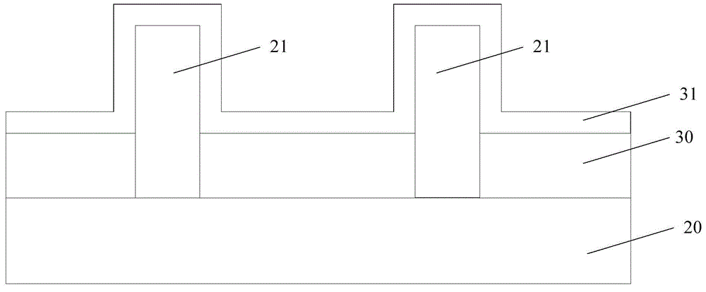
[0034] Please refer to figure 2 , in one embodiment of the present invention, after forming the fin 21 on the semiconductor substrate 20 and the isolation layer 30, a gate structure (not shown) across the fin is formed, and then the isolation layer 30. After the dielectric layer 31 is formed on the surface of the fin 21 and the gate structure, it is a schematic cross-sectional view along the length direction of the fin 21 on both sides of the gate structure.

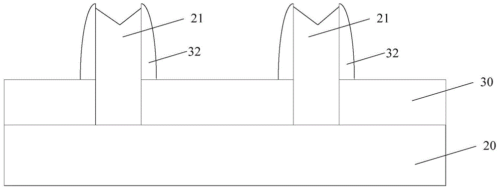
[0035] Please refer to image 3 , using an anisotropic etching process to etch the dielectric layer 31 to expose the top surfaces of the fins 21 on both sides of the gate structure, and form sidewalls 32 covering the sidewall surfaces of the fins 21 .

[0036] In the actual process, the inventors found that after removing the dielectric layer 31 at...


PUM


Abstract

A formation method of a semiconductor structure comprises the following steps of providing a semiconductor substrate; forming a fin portion on the semiconductor substrate; forming an isolation layer on the semiconductor substrate, wherein a surface of the isolation layer is lower than a top surface of the fin portion and covers a side wall of parts of the fin portion; forming a dielectric layer on a fin portion surface; forming a sidewall of the dielectric layer covering a fin portion sidewall surface; taking the side wall as a mask layer, using a wet etching process to etch the dielectric layer so that the top surface of the fin portion is exposed. By using the method, damages to the fin portion, which is generated through using dry etching, can be reduced, which is good for subsequent epitaxial growth; and performance of the formed semiconductor structure is increased.

Description

technical field [0001] The invention relates to the technical field of semiconductors, in particular to a method for forming a semiconductor structure. Background technique [0002] With the continuous development of semiconductor process technology, process nodes are gradually reduced, and gate-last (gate-last) process has been widely used to obtain an ideal threshold voltage and improve device performance. However, when the feature size of the device is further reduced, even if the gate-last process is adopted, the structure of the conventional MOS field effect transistor can no longer meet the requirements for device performance. As a multi-gate device, the fin field effect transistor (FinFET) has relatively high High integration, high control of short channel effect, can get extensive attention. [0003] figure 1 It is a schematic diagram of a three-dimensional structure of a fin field effect transistor in the prior art. [0004] Such as figure 1 As shown, it include...

Claims


Application Information

Patent Timeline
Patent Type & Authority Applications(China)
IPC IPC(8): H01L21/336
Inventor 禹国宾
Owner SEMICON MFG SOUTH CHINA CORP
Why Eureka
Try Eureka