Semi-floating gate device and formation method therefor

A semi-floating gate device and floating gate technology, applied in semiconductor devices, semiconductor/solid-state device manufacturing, electrical components, etc., can solve the problems of unstable performance and poor reliability of semi-floating gate devices, and achieve increased contact area and improved performance effect

Active Publication Date: 2016-02-17
SEMICON MFG INT (SHANGHAI) CORP
View PDF5 Cites 13 Cited by
  • Summary
  • Abstract
  • Description
  • Claims
  • Application Information

AI Technical Summary

Problems solved by technology

[0006] However, the semi-floating gate devices formed by the prior art have unstable performance and poor reliability

Method used


Image

  • Semi-floating gate device and formation method therefor
  • Semi-floating gate device and formation method therefor
  • Semi-floating gate device and formation method therefor

Examples


Embodiment Construction

[0037] As mentioned in the background, the semi-floating gate device formed in the prior art has unstable performance and poor reliability.

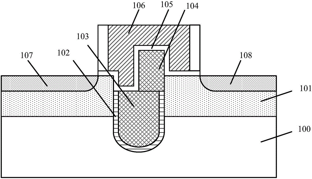
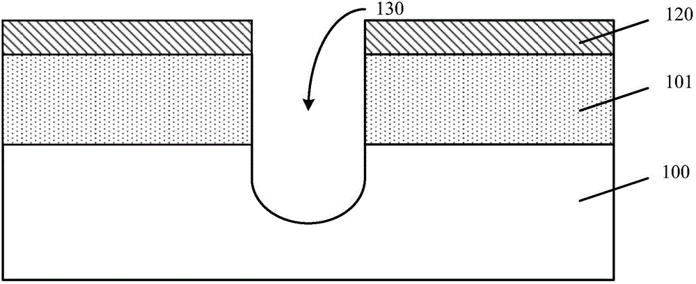
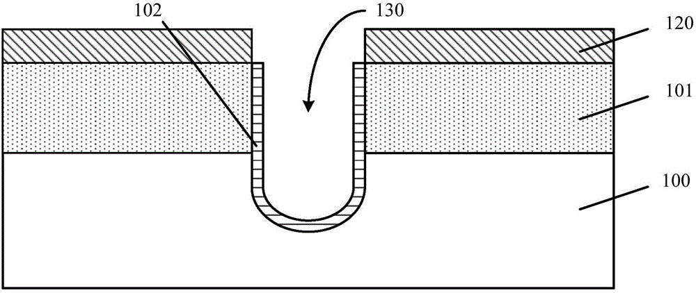
[0038] Please refer to figure 1 , figure 1 It is a schematic cross-sectional structure diagram of a semi-floating gate crystal device according to an embodiment of the present invention, including: a substrate 100 having a doped well region 101 within the doped well region 101 having first dopant ions A trench (not shown) located in the substrate 100, the bottom of the trench is lower than the bottom of the doped well region 101; a gate dielectric layer located on the sidewall and bottom surface of the trench 102, the top of the gate dielectric layer 102 is lower than the top of the trench; the first floating gate layer 103 on the surface of the gate dielectric layer 102 in the trench, the surface of the first floating gate layer 103 is in contact with the gate The top of the dielectric layer 102 is flush; the second floating gate laye...


PUM


Abstract

A semi-floating gate device and a formation method therefor are disclosed. The formation method comprises the steps of providing a substrate, wherein the substrate is provided with a first well region; forming a groove in the substrate, wherein the bottom of the groove is lower than that of the first well region; forming a first dielectric layer on the surfaces of the side wall and the bottom of the groove; forming a floating gate layer on the surface of the first dielectric layer in the groove and the surface of the substrate, wherein the surface of the floating gate layer is higher than that of the substrate; the doping types in the floating gate layer and the first well region are opposite; etching a part of the floating gate layer to form a floating gate, wherein the floating gate comprises a first structure positioned in the groove, and a second structure positioned on the partial surface of the first structure; the second structure is in contact with a partial first well region on one side of the groove; the second structure exposes the top of the first dielectric layer that is positioned on the surface, on the other side of the groove, of the side wall; forming a second dielectric layer on the surface of the floating gate, wherein the second dielectric layer is connected with the first dielectric layer exposed by the floating gate; and forming a control gate on the surface of the second dielectric layer. The performance of the formed semi-floating gate device is improved.

Description

technical field [0001] The invention relates to the technical field of semiconductor manufacturing, in particular to a semi-floating gate device and a forming method thereof. Background technique [0002] In the current semiconductor industry, a storage device is an important part of a digital circuit, and a flash memory (flash memory) memory, as a nonvolatile memory (Nonvolatile Memory, NVM), has been rapidly developed. The main feature of flash memory is that it can keep stored information for a long time without power on, so it is widely used in various memories that urgently need to store data that will not disappear due to power interruption, and that require repeated reading and writing of data. Moreover, flash memory has the advantages of high integration, fast access speed, easy erasing and rewriting, etc., so it has been widely used in many fields such as microcomputers and automatic control. Therefore, how to improve the performance of the flash memory and reduce ...

Claims


Application Information

Patent Timeline
Patent Type & Authority Applications(China)
IPC IPC(8): H01L21/336H01L21/28H01L29/788H01L29/423
Inventor 王文博卜伟海康劲
Owner SEMICON MFG INT (SHANGHAI) CORP
Why Eureka
Try Eureka