
Method for improving STI and FG poly filling hole process window simultaneously

A process window and cavity filling technology, which is applied in the fields of electrical components, semiconductor/solid-state device manufacturing, circuits, etc., can solve the problems of unrecorded EM combination AA and silicon nitride morphology adjustment, and achieve the effect of reducing cost and debugging cycle

Inactive Publication Date: 2016-02-17
SHANGHAI HUALI MICROELECTRONICS CORP
View PDF5 Cites 0 Cited by
  • Summary
  • Abstract
  • Description
  • Claims
  • Application Information

AI Technical Summary

Problems solved by technology

[0005] The above two patents do not record the combination of AA and silicon nitride morphology adjustment through lithography size EM, and wet chemical solvent etching after FGCMP, and finally use scanning mirror to quickly and effectively debug and observe STI and FG filling voids Technical characteristics of the process window

Method used


Image

  • Method for improving STI and FG poly filling hole process window simultaneously
  • Method for improving STI and FG poly filling hole process window simultaneously
  • Method for improving STI and FG poly filling hole process window simultaneously

Examples


Embodiment Construction

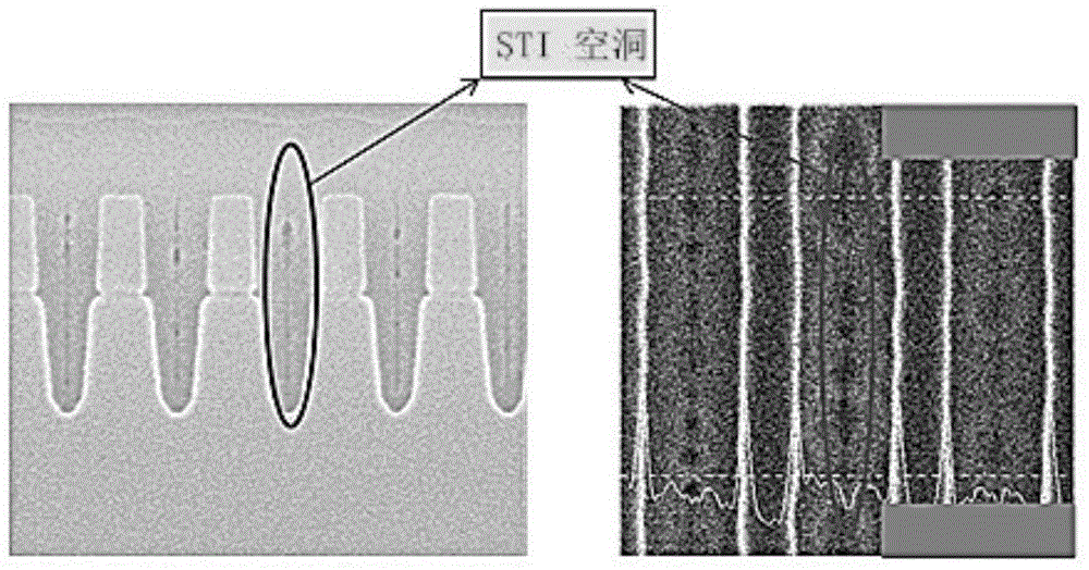
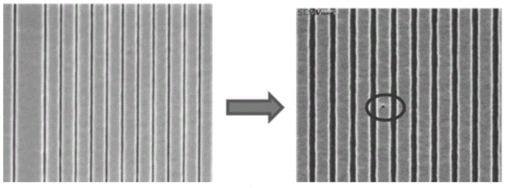
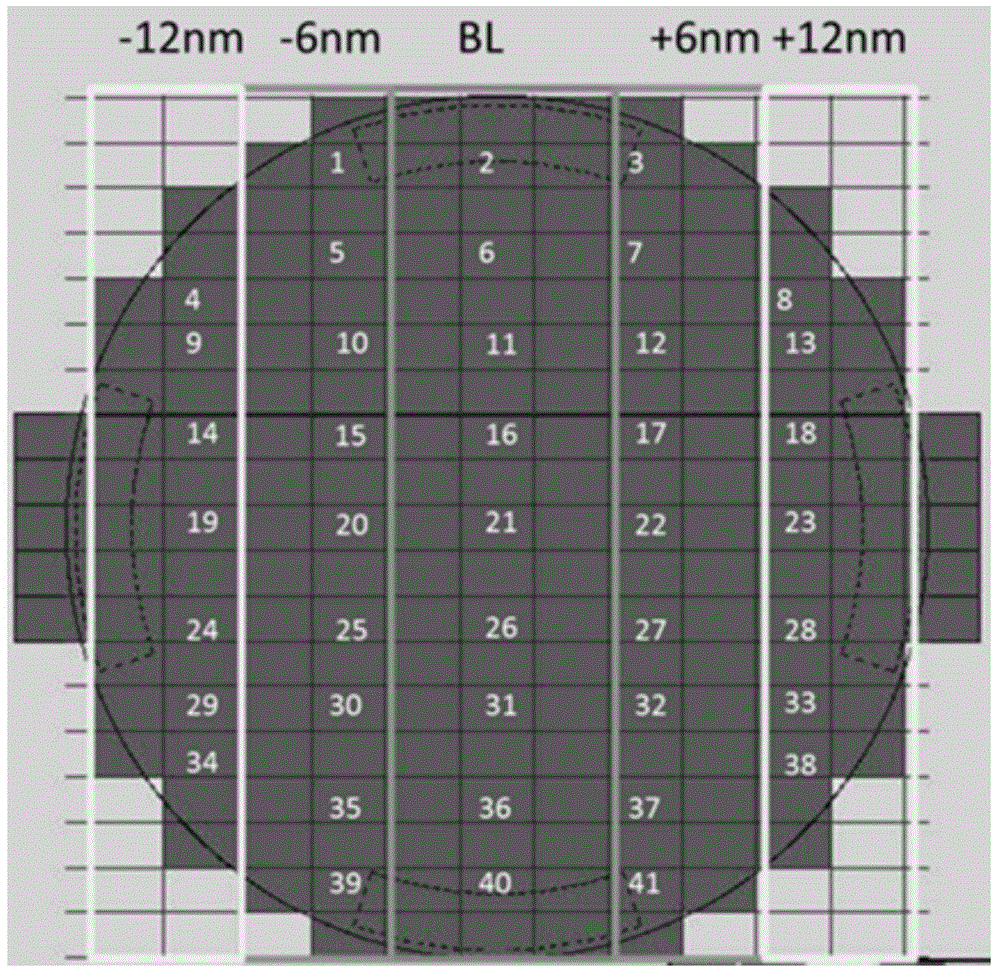
[0027] The present invention provides a method for simultaneously improving the process window of STI and FGPoly filling voids, which can be applied in the field of semiconductor production, and can preferably be applied to technologies such as 65 / 55nm and 45 / 40nm technology nodes, and applied to technology platforms such as MemoryFlasheFlash And in the technical module of PIE, when this method is used, the active region and the morphology of silicon nitride can be adjusted by lithography size EM, combined with FGCMP post-wet chemical solvent etching, and then scanning electron microscopy can be used to quickly and effectively Debugging and observing the process window of STI and FG filling voids accurately, which greatly reduces the cost and debugging cycle compared with the single-step traditional method.

[0028] The core idea of ​​the present invention is to first define the size of the active area from small to large by using the active area photolithography process EM, an...


PUM


Abstract

The invention provides a method for improving an STI and FG poly filling hole process window simultaneously. The method comprises: a flash memory device is designed; ascending-order-based active region dimensions are defined from left to right by using an active region photoetching process; an isolated shallow slot opening morphology and a silicon nitride blocking thickness are adjusted and adjusted results are combined with active region dimensions; floating gate planarization process is carried out on a combined wafer and wet etching is carried out on the surface of the combined wafer; and observation and debugging are carried out by using a scanning electron microscope to search a proper STI and FG filling hole process window. For the planarization process, a chemical mechanical grinding process is used; and the isolated shallow slot opening appearance is in a taper shape; and the STI filling hole is adjusted by adjusting the opening morphology of the isolated shallow slot and the FG poly filling hole is adjusted by adjusting the silicon nitride thickness.

Description

technical field [0001] The invention relates to the field of semiconductors, in particular to a method for simultaneously improving the process window of STI and FGPoly filling holes. Background technique [0002] In the development of self-aligned floating gate process flash memory products at 65nm and below nodes, due to the specification requirements, the size of the flash memory array STI and AA (Active Area: active area) is small, and the small size of STI will make the shallow trench isolation silicon oxide Filling produces voids, but at the same time, the larger the size of STI and the smaller the size of AA, it is easy to generate voids filled with floating gate polysilicon, which determines that it is quite complicated and difficult to find a balanced process window between the two , the current monitoring and debugging method routinely used in the process of process development is to determine the process window by single-step debugging and then scanning electron m...

Claims


Application Information

Patent Timeline
Patent Type & Authority Applications(China)
IPC IPC(8): H01L21/8247H01L21/66H01L21/762H01L21/28
Inventor 殷冠华陈广龙
Owner SHANGHAI HUALI MICROELECTRONICS CORP
Learn More