BCD device and manufacturing method thereof
A manufacturing method and device technology, applied in the field of BCD devices and their manufacturing, can solve the problems of low efficiency and high lithography cost
- Summary
- Abstract
- Description
- Claims
- Application Information
AI Technical Summary
Problems solved by technology
Method used
Image

Examples
Embodiment Construction
[0155] The present invention will be further described below with reference to specific embodiments and drawings, but the protection scope of the present invention should not be limited by this.
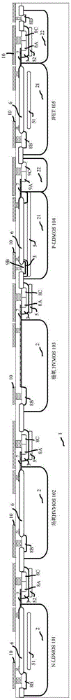
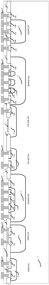
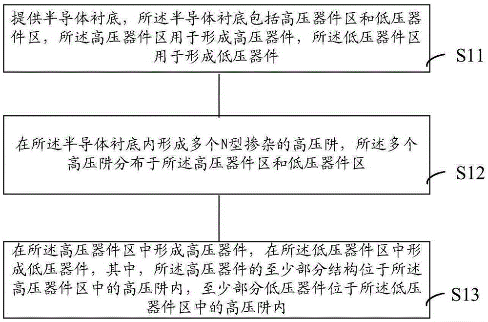
[0156] In the BCD device of this embodiment, the semiconductor substrate includes a high-voltage device area and a low-voltage device area, wherein one or more N-type doped high-voltage wells are formed in both the high-voltage device area and the low-voltage device area, and at least part of the high-voltage device The composition structure is formed in the high-voltage well in the high-voltage device region, and at least part of the low-voltage devices are formed in the high-voltage well in the low-voltage device region.
[0157] Preferably, each high-voltage well in the high-voltage device region and the low-voltage device region can be formed using the same photolithography and ion implantation process steps, so as to save the number of photolithography and reduce the cost. In additio...
PUM
 Abstract
Description
Claims
Application Information