Top-gate type thin film transistor and manufacturing method thereof

A thin-film transistor, top-gate technology, used in transistors, semiconductor/solid-state device manufacturing, electrical components, etc., can solve problems such as threshold voltage shift, TFT characteristic change, restricting the application of oxide TFT, etc., to improve stability, increase The effect of lithography times

Active Publication Date: 2019-06-28
SOUTH CHINA UNIV OF TECH
View PDF5 Cites 2 Cited by
  • Summary
  • Abstract
  • Description
  • Claims
  • Application Information

AI Technical Summary

Problems solved by technology

However, when oxide TFT devices work on the display screen, due to the effects of light, heat and other conditions in the actual working environment, long-term operation will lead to changes in TFT characteristics, such as threshold voltage drift and photostability deterioration. However, The prior art cannot solve the problem of how to adjust the threshold voltage of oxide TFTs and improve the light stability of TFT devices, which also seriously restricts the application of oxide TFTs in flat panel display devices.

Method used


Image

  • Top-gate type thin film transistor and manufacturing method thereof
  • Top-gate type thin film transistor and manufacturing method thereof
  • Top-gate type thin film transistor and manufacturing method thereof

Examples


Embodiment

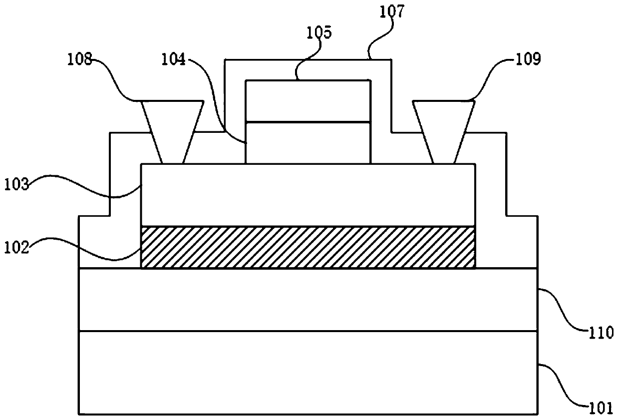
[0036] figure 1 For a schematic structural diagram of a top-gate thin film transistor provided in an embodiment of the present invention, refer to figure 1 , the top-gate thin film transistor includes a substrate 101, an oxide modification layer 102, an active layer 103, a gate insulating layer 104, a gate 105, a passivation layer 107, a source 108 and a drain 109;

[0037] The oxide modification layer 102 is disposed between the substrate 101 and the active layer 103 .

[0038] The threshold voltage of a top-gate TFT is usually related to the interface trap state density between the active layer and the insulating layer, while the charge trap density is mainly determined by the quality of the interface between the semiconductor layer and the insulating layer. When the material purity is low or the contact quality of the semiconducting layer / insulating layer interface is poor, the device usually has a large trap density. The charge traps existing at the interface will trap ca...


PUM


Abstract

The invention discloses a top-gate type thin film transistor. The top-gate type thin film transistor comprises a substrate, an oxide modification layer, an active layer, a grid insulation layer, a grid electrode, a passivation layer, a source electrode and a drain electrode. The oxide modification layer is arranged between the substrate and the active layer. The oxide modification layer can adjustthe performance of the top-gate type thin film transistor, so as to achieve the effect of improving the stability. Meanwhile, the oxide modification layer and the active layer can be patterned at thesame time, and the photoetching frequency can be not increased, thereby improving the performance of the top gate type thin film transistor on the premise that the photoetching cost is not increased.

Description

technical field [0001] Embodiments of the present invention relate to semiconductor manufacturing technology, and in particular to a top-gate thin film transistor and a manufacturing method thereof. Background technique [0002] In recent years, with the rapid development of Flat Panel Display (FPD), especially Organic Light-Emitting Diode (OLED), the backplane technology of thin-film transistor (ThinFilm Transistor, TFT), which is the core technology, has also undergoing profound changes. Metal oxide semiconductors have the advantages of high carrier mobility (1-100cm2 / Vs), transparency to visible light, simple process, low cost, and high uniformity in large areas. In the field of TFT substrates for flat panel displays, there are alternatives to traditional silicon The trend of thin film transistors prepared by advanced technology has become the focus of industry and academia. However, when oxide TFT devices work on the display screen, due to the effects of light and heat...

Claims


Application Information

Patent Timeline
Patent Type & Authority Applications(China)
IPC IPC(8): H01L29/786H01L21/336
Inventor 徐苗李美灵李民张伟王磊邹建华陶洪彭俊彪
Owner SOUTH CHINA UNIV OF TECH
Why Eureka
Try Eureka