Embedded gate top surface contact field effect transistor structure and manufacturing method thereof

A field effect transistor, top surface technology, applied in the direction of semiconductor/solid state device manufacturing, semiconductor devices, electrical components, etc., to achieve the effect of increasing the processing process window, reducing the lithography alignment process process, and simplifying the processing process

Active Publication Date: 2021-08-20
深圳真茂佳半导体有限公司
View PDF7 Cites 2 Cited by
  • Summary
  • Abstract
  • Description
  • Claims
  • Application Information

AI Technical Summary

Problems solved by technology

[0005] The main purpose of the present invention is to provide a field effect transistor structure with buried gate top surface contact. Under the concept of contact hole partition processing, the main progress lies in the innovative transistor structure with source / drain and gate interleaved and stacked Solve the problem that the area of ​​the mesa area of ​​the field effect transistor is affected by the reduction of the area of ​​the contact hole, and can increase the arrangement density of the embedded gate in the mesa area to further reduce the gate pitch

Method used


Image

  • Embedded gate top surface contact field effect transistor structure and manufacturing method thereof
  • Embedded gate top surface contact field effect transistor structure and manufacturing method thereof
  • Embedded gate top surface contact field effect transistor structure and manufacturing method thereof

Examples


Embodiment Construction

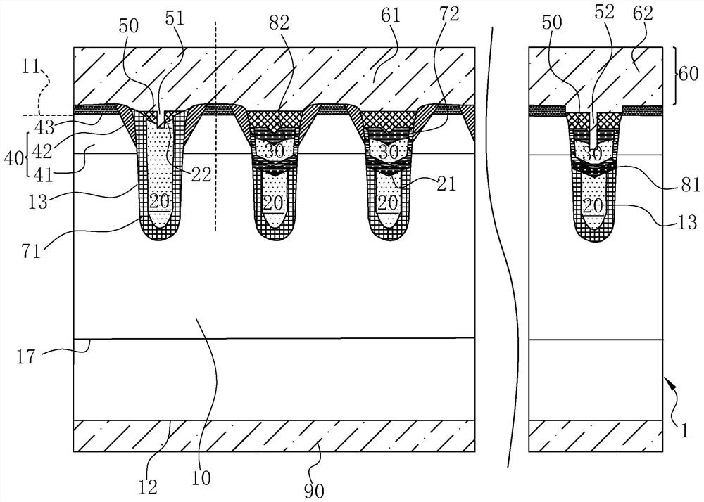
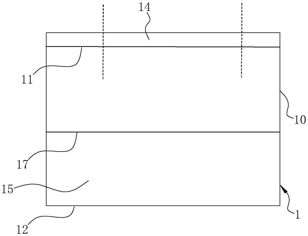
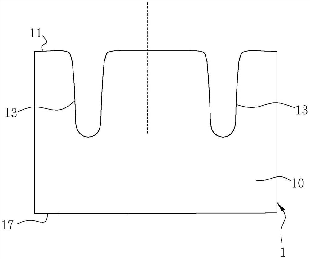
[0080] The technical solutions in the embodiments of the present invention will be clearly and completely described below in conjunction with the accompanying drawings in the embodiments of the present invention. Apparently, the described embodiments are only part of the embodiments for understanding the inventive concepts of the present invention, and cannot represent All the embodiments are not explained as the only embodiment. Based on the embodiments of the present invention, all other embodiments obtained by persons of ordinary skill in the art on the premise of understanding the inventive concepts of the present invention fall within the protection scope of the present invention.

[0081] It should be noted that if there is a directional indication (such as up, down, left, right, front, back...) in the embodiment of the present invention, the directional indication is only used to explain the relationship between the components in a certain posture. If the specific postu...


PUM


Abstract

The invention relates to an embedded gate top surface contact field effect transistor structure and a manufacturing method thereof. The transistor comprises a drain epitaxial layer, a surface metal layer which is located on the top layer and can be divided into a source metal pad and a gate metal pad, and an embedded source extension inverted fin and a gate which are located in the drain epitaxial layer. The gate is aligned to the source extension inverted fin, and symmetrical channels which are connected in parallel from the surface metal layer to the interior of the drain epitaxial layer in pairs are formed on the two sides of the gate respectively; by means of the design that the embedded source extension inverted finand the gate are in the same groove and are not in the same area, the source metal pad and the gate metal pad are individually conducted outside the mesa area, and the condition that the mesa area needs to be provided with a contact hole is avoided. The field effect transistor architecture provided by the invention has the effect of reducing the gate trench pitch to improve the electron current density.

Description

technical field [0001] The invention relates to the technical field of semiconductor transistors, in particular to a field-effect transistor structure and a manufacturing method thereof with embedded gate top surface contact. Background technique [0002] As the key and important device of the semiconductor chip, the field effect transistor structure has a variety of structures, mainly including the following types: FinFET fin field effect transistor, JFET junction field effect transistor, surface field effect transistor, tunneling field effect transistor Transistors trench gate field effect transistor, split gate field effect transistor and super junction field effect transistor. Among them, the structure of FinFET fin field effect transistor, JFET junction field effect transistor, surface field effect transistor and tunneling field effect transistor is to design the source contact and drain contact on the same surface of the semiconductor substrate. With the trend of thin...

Claims


Application Information

Patent Timeline
Patent Type & Authority Applications(China)
IPC IPC(8): H01L29/417H01L29/423H01L29/06H01L29/08H01L29/78H01L21/28H01L21/027H01L21/336
CPCH01L29/7827H01L29/66666H01L29/0649H01L29/0847H01L29/41741H01L29/42356H01L29/4236H01L29/42364H01L29/401H01L21/0274H01L29/0684
Inventor 任炜强
Owner 深圳真茂佳半导体有限公司
Why Eureka
Try Eureka