bcd device and manufacturing method thereof

A manufacturing method and device technology, applied in the field of BCD devices and its manufacturing, can solve the problems of low efficiency and high cost of lithography

Active Publication Date: 2019-08-16
HANGZHOU SILAN MICROELECTRONICS
View PDF9 Cites 0 Cited by
  • Summary
  • Abstract
  • Description
  • Claims
  • Application Information

AI Technical Summary

Problems solved by technology

Among them, the low-voltage well and the high-voltage well need to be formed by different lithography processes, resulting in high lithography costs and low efficiency.

Method used


Image

  • bcd device and manufacturing method thereof
  • bcd device and manufacturing method thereof
  • bcd device and manufacturing method thereof

Examples


Embodiment Construction

[0155] The present invention will be further described below in conjunction with specific embodiments and accompanying drawings, but the protection scope of the present invention should not be limited thereby.

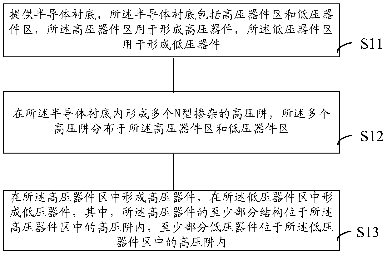
[0156] In the BCD device of this embodiment, the semiconductor substrate includes a high-voltage device region and a low-voltage device region, wherein one or more N-type doped high-voltage wells are formed in both the high-voltage device region and the low-voltage device region, and at least part of the high-voltage device The compositional structure is formed in the high voltage well in the high voltage device region, and at least part of the low voltage device is formed in the high voltage well in the low voltage device region.

[0157] Preferably, each high-voltage well in the high-voltage device region and the low-voltage device region can be formed by using the same photolithography and ion implantation process steps, so as to save the number of times of photolith...


PUM


Abstract

The invention provides a BCD (Bipolar-CMOS-DMOS) device and a manufacturing method thereof. The BCD device comprises a semiconductor substrate and a plurality of N type doped high voltage wells, wherein the semiconductor substrate includes a high voltage device area and a low voltage device area; the high voltage device area is used for forming high voltage devices; the low voltage device area is used for forming low voltage devices; the plurality of N type doped high voltage wells are distributed in the high voltage device area and the low voltage device area; at least part of the component structures of the high voltage devices are formed in the high voltage wells of the high voltage device area; and at least part of the low voltage devices are formed in the high voltage wells of the low voltage device area. The BCD device and the manufacturing method thereof can reduce the frequency for the photoetching process, and can be conductive to cost reduction and efficiency improvement.

Description

technical field [0001] The invention relates to BCD technology, in particular to a BCD device and a manufacturing method thereof. Background technique [0002] BCD (Bipolar-CMOS-DMOS) technology is a monolithic integration process technology. This technology can make diodes (Bipolar), complementary metal-oxide-semiconductor field-effect transistors (CMOS) and double-diffused metal-oxide-semiconductor field-effect transistors (DMOS) devices on the same chip, so it is called BCD technology for short. [0003] High-voltage BCD technology generally refers to BCD technology with a device withstand voltage above 100V. High-voltage BCD technology is currently widely used in AC-DC power supplies, LED drivers and other fields, and generally requires devices to withstand voltages ranging from 500V to 800V. [0004] In the prior art, a BCD device is often integrated with a high-voltage device and a low-voltage device. For example, the high-voltage device may be an LDMOS device, a hig...

Claims


Application Information

Patent Timeline
Patent Type & Authority Patents(China)
IPC IPC(8): H01L27/06H01L21/8249
CPCH01L21/8249H01L27/06
Inventor 姚国亮张邵华吴建兴
Owner HANGZHOU SILAN MICROELECTRONICS
Why Eureka
Try Eureka