1T1R and 1R resistive random access memory integrated structure and implement method thereof

A resistive memory, 1.1T1R technology, applied in the field of microelectronics, can solve the problem of high processing cost

Active Publication Date: 2013-12-11
PEKING UNIV
View PDF4 Cites 2 Cited by
  • Summary
  • Abstract
  • Description
  • Claims
  • Application Information

AI Technical Summary

Problems solved by technology

[0004] In the prior art and method, in the process of manufacturing the above-mentioned 1R and 1T1R,...

Method used


Image

  • 1T1R and 1R resistive random access memory integrated structure and implement method thereof
  • 1T1R and 1R resistive random access memory integrated structure and implement method thereof
  • 1T1R and 1R resistive random access memory integrated structure and implement method thereof

Examples


Embodiment 1

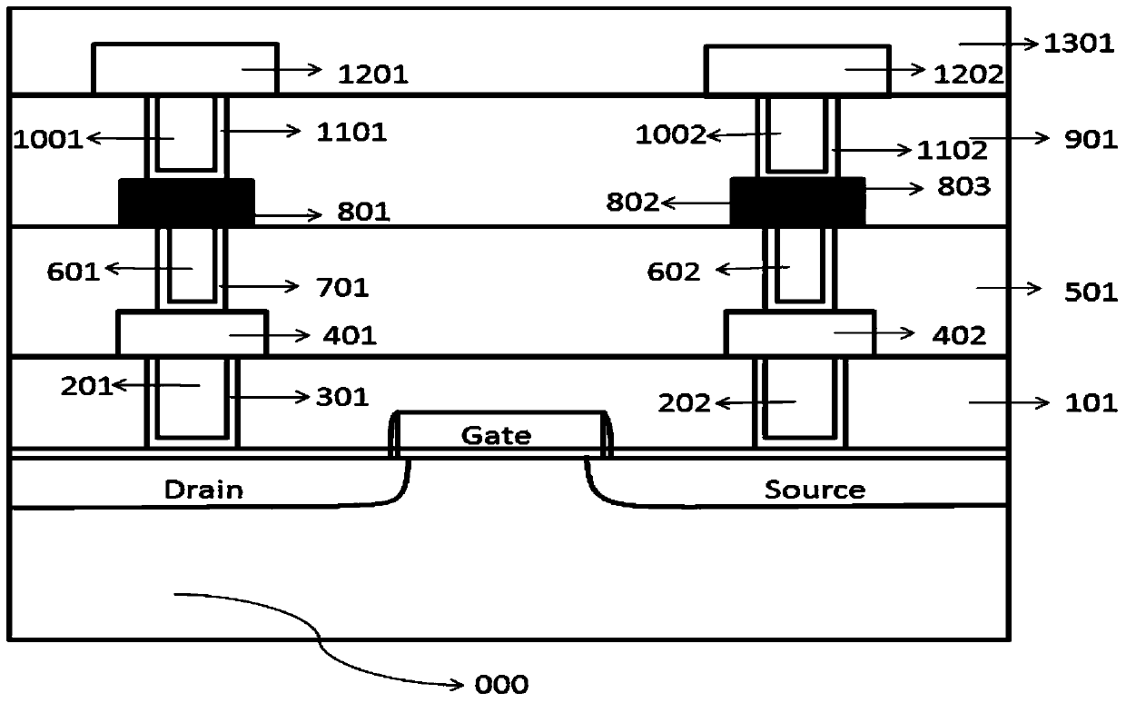
[0049] Embodiment 1 of the present invention provides an integrated structure of 1T1R and 1R resistive memory, and the composition structure diagram is as follows figure 1 As shown, it specifically includes: substrate transistor 000, first layer metal pre-dielectric 101, first layer plugs 201 and 202, first layer metal 401 and 402, second layer interlayer dielectric 501, second layer plugs 601 and 602 , MIM structure layers 801, 802 and 803, a third layer of interlayer dielectric 901, a third layer of plugs 1001 and 1002, a second layer of metal 1201 and 1202, and a passivation layer 1301.

[0050] In the integrated structure of 1T1R and 1R resistive memory, a resistive memory with a MIM structure layer is fabricated on the drain and source of the substrate transistor respectively, thereby realizing the integration of 1T1R and 1R. The integration of the 1T1R structure and the 1R structure facilitates the comparison of the characteristics of the RRAM in the two structures, and ...

Embodiment 2

[0057] Embodiment 2 of the present invention provides a method for realizing the integrated structure of the 1T1R and 1R resistive variable memory, including: fabricating the resistive variable memory at the source and drain of the substrate transistor at the same time, and realizing the connection between the substrate transistor and the drain through the drain and source A series connection of resistive memory.

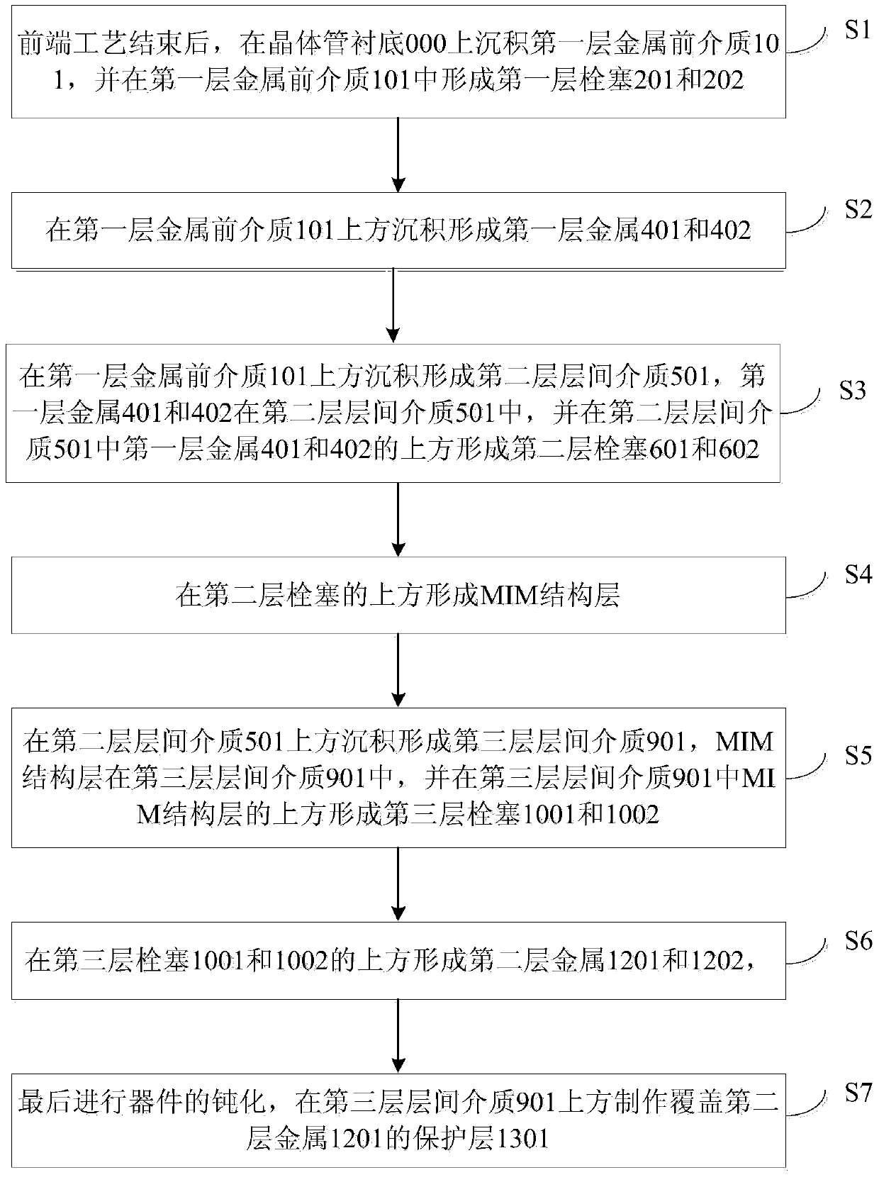
[0058] The steps of fabricating the resistive variable memory at the source and drain of the substrate transistor are as follows: figure 2 As shown, it specifically includes the following steps:

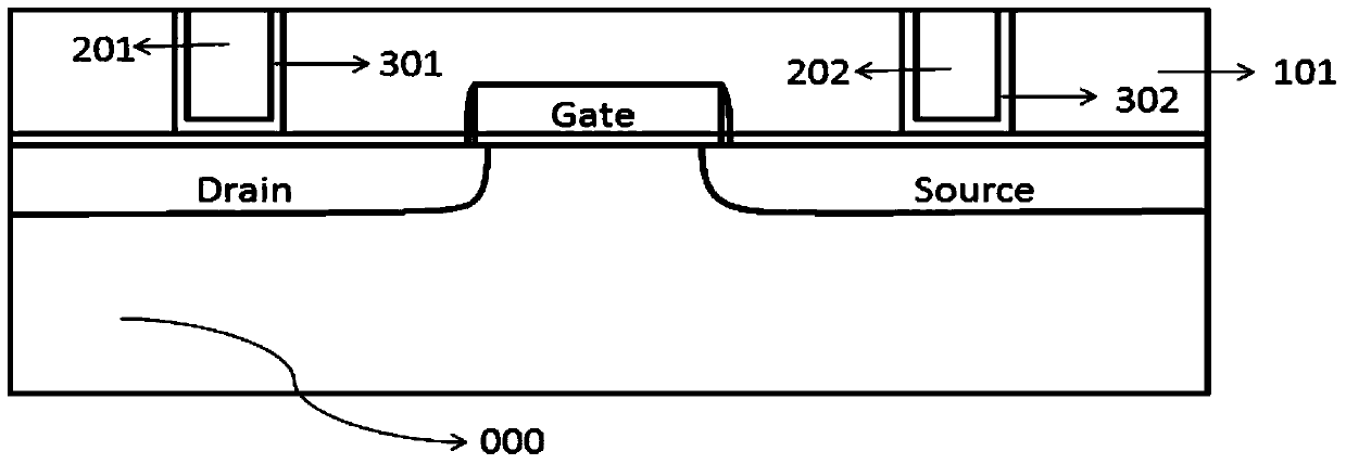
[0059] Step S1, after the front-end process is completed, the first layer of pre-metal dielectric 101 is deposited on the substrate transistor 000, and the first layer of plugs 201 and 202 are formed in the first layer of pre-metal dielectric 101. The first layer of plugs 201 and 202 are respectively Formed on the drain Drain and the source Source of the substrate transi...


PUM

PropertyMeasurementUnit
Thicknessaaaaaaaaaa
Thicknessaaaaaaaaaa

Abstract

The invention discloses a 1T1R and 1R resistive random access memory integrated structure and an implement method thereof. Resistive random access memory structures with MIM structures are manufactured on a drain electrode and a source electrode of an original substrate transistor respectively at the same time, a first layer of metal front medium, a first layer of plug, a first layer of metal, a second layer of inter-layer medium, a second layer of plug, an MIM structure layer, a third layer of inter-layer medium, a third layer of plug, a second layer of metal and a passivation layer are sequentially and respectively formed above the drain electrode and the source electrode of the substrate transistor, and the substrate transistor is connected with resistive random access memories in series. The resistive random access memory in the 1T1R structure and the resistive random access memory in the 1R structure are manufactured at the same time, the technological conditions are completely the same, the photo-etching times can be reduced, manufacturing cost is reduced, meanwhile, the 1T1R structure and the 1R structure are integrated, the characteristics of the resistive random access memories in the two structures can be compared conveniently, and the effect on the changing characteristic of a device from the current overshoot can be studied.

Description

technical field [0001] The invention relates to the technical field of microelectronics, in particular to an integrated structure of 1T1R and 1R resistive variable memory and a realization method thereof. Background technique [0002] Resistive Random Access Memory (RRAM) is considered to be a strong competitor for the next generation of new memory because of its high density, low cost, fast access speed and breakthrough technology development. Resistive variable memory uses the characteristics of the resistance of the storage medium to reversibly switch between low-resistance state and high-resistance state under the action of electrical signals to store signals. The process of changing from high-resistance state to low-resistance state is called set. The process of transitioning to a high-impedance state is called reset. There are many kinds of storage media, including binary transition metal oxides, perovskite compounds, solid electrolytes, and organic materials. Transi...

Claims


Application Information

Patent Timeline
IPC IPC(8): H01L27/24H01L27/10G11C13/00
Inventor 刘力锋张伟兵李悦韩德栋王漪刘晓彦康晋锋张兴
Owner PEKING UNIV
Why Eureka
Try Eureka