Method for preparing contact electrode of infrared detector chip

An infrared detector and contact electrode technology, applied in the field of infrared detectors, can solve the problems of damaged chips and complex electrode preparation process, and achieve the effects of reducing process steps, reducing the number of lithography, and reducing the difficulty of the process

Inactive Publication Date: 2020-07-10
11TH RES INST OF CHINA ELECTRONICS TECH GROUP CORP
View PDF3 Cites 2 Cited by
  • Summary
  • Abstract
  • Description
  • Claims
  • Application Information

AI Technical Summary

Problems solved by technology

[0004] An embodiment of the present invention provides a method for preparing a contact electrode of an infrared detector chip, which is used to solve the problems of complicated electrode preparation process and chip damage in the prior art

Method used


Image

  • Method for preparing contact electrode of infrared detector chip
  • Method for preparing contact electrode of infrared detector chip
  • Method for preparing contact electrode of infrared detector chip

Examples


preparation example Construction

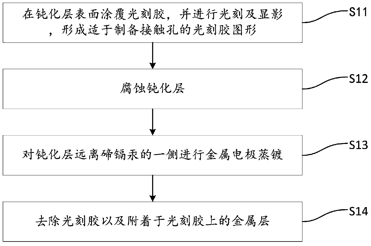
[0035] The embodiment of the present invention proposes a method for preparing a contact electrode of an infrared detector chip, such as figure 1 As shown, the method includes:

[0036] S11, coating a photoresist on the surface of the passivation layer, and performing photolithography and development to form a photoresist pattern suitable for preparing contact holes.

[0037] Such as figure 2 As shown, numeral 10 denotes a substrate (such as a cadmium zinc telluride substrate), numeral 20 denotes mercury cadmium telluride, numeral 30 denotes a passivation layer, and numeral 40 denotes a photoresist.

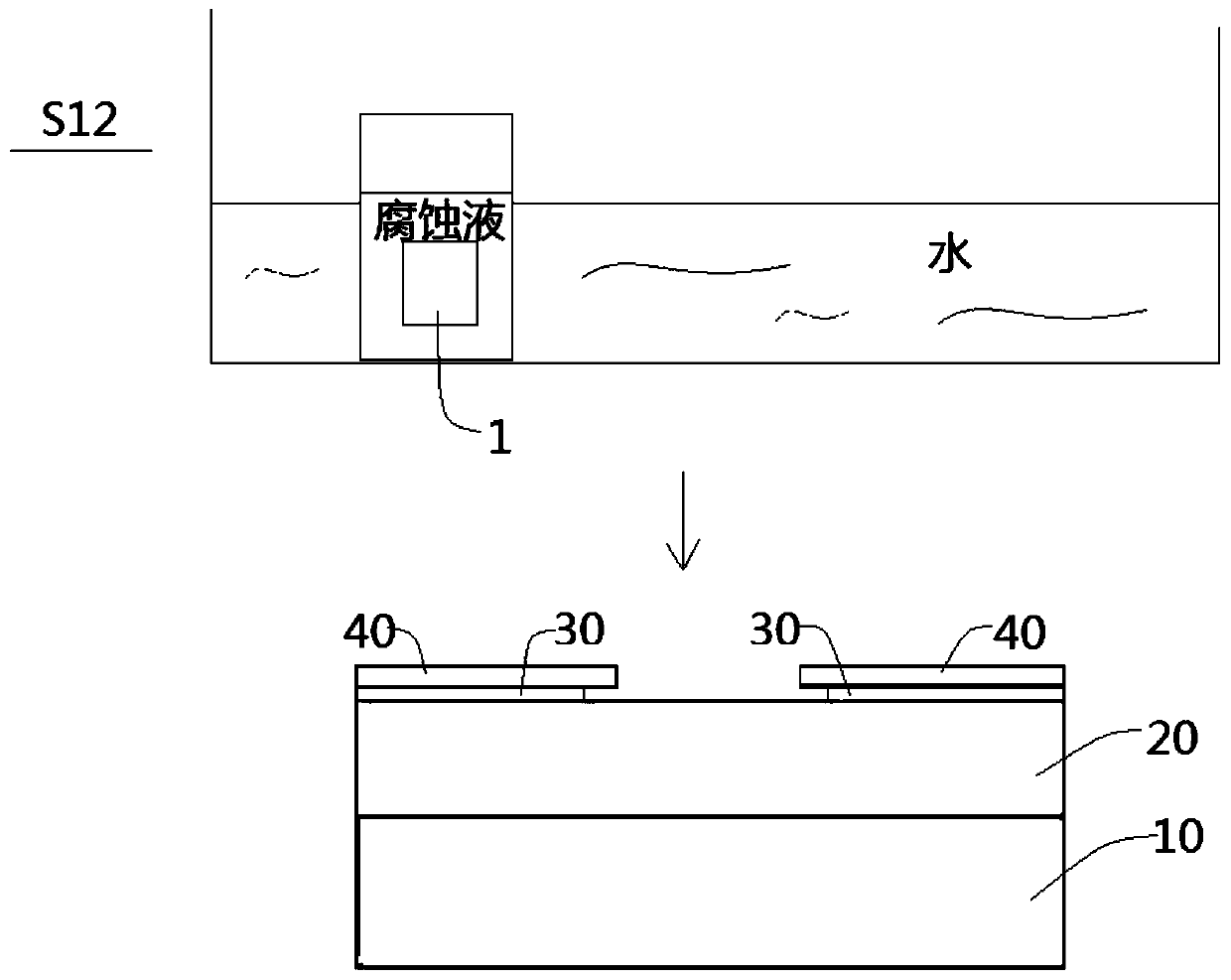
[0038] S12, corrosion passivation layer;

[0039] It will be appreciated that portions of the passivation layer not coated with photoresist may be etched away. Due to the omnidirectional nature of the corrosion, the part of the passivation layer covered by the photoresist will also be corroded by a small amount, forming a lateral corrosion area. Such as image 3 As shown, a...

Embodiment 1

[0063] Such as Figure 6 As shown, the contact electrode preparation method of the infrared detector chip of the embodiment of the present invention includes:

[0064] S21, using corrosion-resistant positive photoresist or negative photoresist with a thickness of 1-4 μm, and obtaining a photoresist pattern of a contact hole through a photolithography and development process.

[0065] S22, use concentrated hydrochloric acid, or a mixed solution of concentrated hydrochloric acid and water (volume ratio: 0.1-10), and use an ultrasonic frequency: 20KHz to 200KHz to ultrasonically corrode the ZnS passivation layer.

[0066] S23, using thermal evaporation technology to sequentially vapor-deposit metal layers Cr and Au, wherein the thickness of Cr is The thickness of Au in A contact metal layer is evaporated onto the chip surface.

[0067] S24, using acetone solution or other organic solvents to dissolve the photoresist, and peel off the metal electrodes.

Embodiment 2

[0069] Such as Figure 7 As shown, the contact electrode preparation method of the infrared detector chip of the embodiment of the present invention includes:

[0070] S31, using corrosion-resistant positive photoresist or negative photoresist with a thickness of 1-4 μm, and obtaining a photoresist pattern of a contact hole through a photolithography and development process.

[0071] S32, use a mixed solution of concentrated hydrochloric acid and concentrated nitric acid, volume ratio: 0.1-10, use ultrasonic frequency: 20KHz-200KHz, ultrasonically corrode the ZnS passivation layer.

[0072] S33, using thermal evaporation technology to sequentially vapor-deposit metal layers Cr and Au, wherein the thickness of Cr is The thickness of Au in A contact metal layer is evaporated onto the chip surface.

[0073] S34, using acetone solution or other organic solvents to dissolve the photoresist, and peel off the metal electrodes.

[0074] By adopting the embodiment of the presen...


PUM

PropertyMeasurementUnit
thicknessaaaaaaaaaa

Abstract

The invention discloses a method for preparing a contact electrode of an infrared detector chip, which comprises the following steps of: coating photoresist on the surface of a passivation layer, photoetching and developing to form a photoresist pattern suitable for preparing a contact hole; corroding the passivation layer; performing metal electrode evaporation on the side, away from tellurium, cadmium and mercury, of the passivation layer; and removing the photoresist and the metal layer attached to the photoresist. By the adoption of the method, a passivation layer corrosion process and anelectrode stripping process are combined, damage to tellurium, cadmium and mercury and the passivation layer in the process is avoided, the number of photoetching times is reduced, process steps are reduced, lateral corrosion of passivation layer corrosion is ingeniously utilized, the stripping process difficulty is greatly reduced, and the rate of finished products is increased.

Description

technical field [0001] The invention relates to the technical field of infrared detectors, in particular to a method for preparing a contact electrode of an infrared detector chip. Background technique [0002] Due to its adjustable wavelength, high quantum efficiency and good device performance, HgCdTe infrared detector has become an important material for high-performance cooled infrared detectors. After decades of development, infrared detectors have developed to the third generation, further expanding the performance and detection capabilities of infrared devices in the direction of large area arrays, long wavelengths, dual-multicolor devices, and high-temperature operating devices. The electrode extraction of the infrared detector is a key step in the preparation of the detector. The electrode preparation process is mainly divided into two steps: opening the passivation layer and electrode extraction. [0003] In related technologies, the opening of the passivation lay...

Claims


Application Information

Patent Timeline
Patent Type & Authority Applications(China)
IPC IPC(8): H01L31/0224H01L31/09H01L31/101H01L31/18
CPCH01L31/0224H01L31/09H01L31/101H01L31/1832Y02P70/50
Inventor 刘世光张轶谭振周立庆
Owner 11TH RES INST OF CHINA ELECTRONICS TECH GROUP CORP
Why Eureka
Try Eureka