
Light distribution structure of light-emitting diode (LED) lamp

A technology for LED lamps and lamps, which is applied in the directions of light sources, light source fixing, and components of lighting devices, etc., can solve the problems of high risk, poor process stability, and enlarged waterproof area, and achieves reduction of light-emitting area, small light-emitting area, and heat dissipation. good effect

Inactive Publication Date: 2016-02-24
苏州艾莱科光电科技有限公司
View PDF4 Cites 1 Cited by
  • Summary
  • Abstract
  • Description
  • Claims
  • Application Information

AI Technical Summary

Problems solved by technology

Glass has the characteristics of high light transmittance, easy to clean and good weather resistance, but the overall cost is high and the process stability is poor. The light transmittance of plexiglass is low and it is easy to yellow; the injection molding process of large plastic lenses is too complicated, the cost is too high, and the dimensional stability is not good. it is good
Small single-particle separated plastic lenses or single-particle conjoined lenses are easy to process and low in cost, but the area occupied is too large, resulting in relatively large PCB aluminum plate area and lamp housing area, high cost, and increased risk of waterproofing area , and the design flexibility of the lamp body is not enough
[0004] Generally speaking, the area occupied by single-particle plastic lenses in the prior art is too large, the overall cost of lamps is high, and the process of single large lenses is complex and poor in stability

Method used


Image

  • Light distribution structure of light-emitting diode (LED) lamp
  • Light distribution structure of light-emitting diode (LED) lamp
  • Light distribution structure of light-emitting diode (LED) lamp

Examples


Embodiment Construction

[0027] The specific implementation manners of the present invention will be further described below in conjunction with the drawings and examples. The following examples are only used to illustrate the technical solution of the present invention more clearly, but not to limit the protection scope of the present invention.

[0028] The technical scheme of concrete implementation of the present invention is:

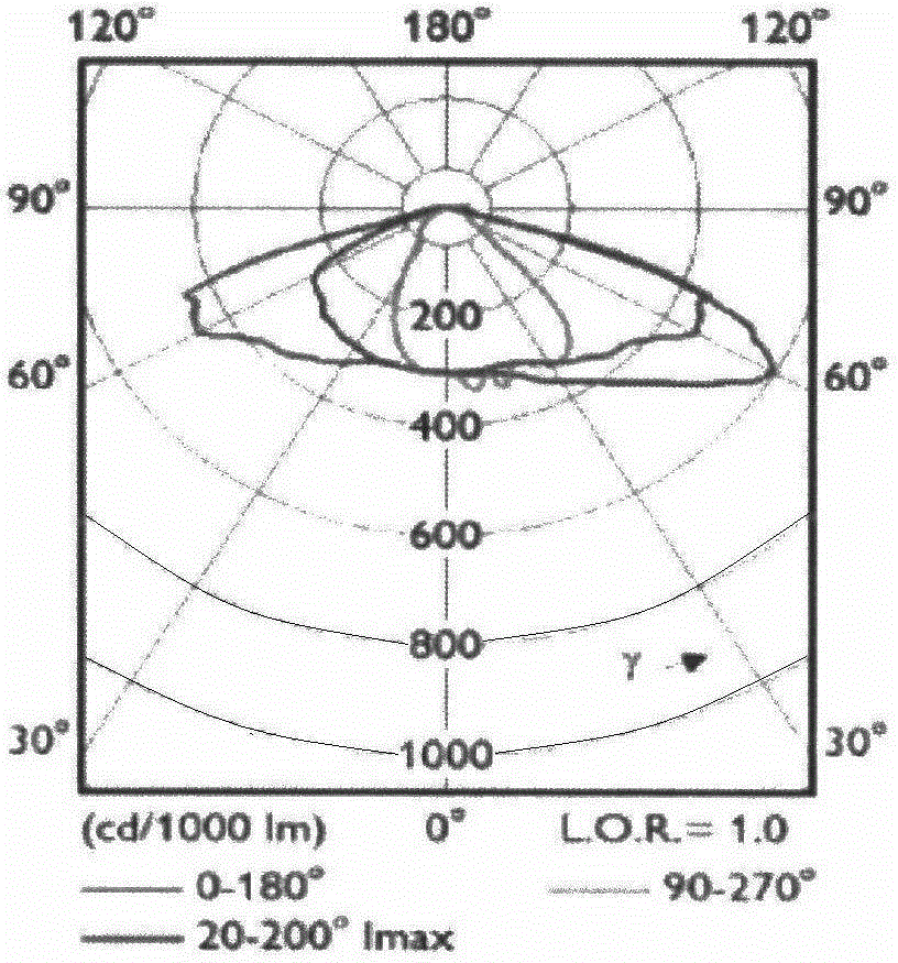
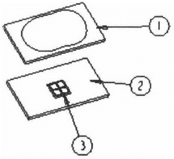
[0029] Such as figure 1 As shown, a light distribution structure of an LED lamp includes: a PCB aluminum substrate 2 welded with a lamp bead group 3, and a plastic lens 1 for covering the lamp bead group 3;

[0030] The lamp bead group 3 is composed of four medium-power 3030 double-crystal lamp beads, and the four lamp beads are distributed in a square shape;

[0031] The plastic lens 1 is provided with a convex surface cover for covering the lamp bead group 3;

[0032] The plastic lens 1 is made of UV-resistant PC material.

[0033] The inner cavity diameter of the co...


PUM

PropertyMeasurementUnit
Thermal conductivityaaaaaaaaaa

Abstract

The invention discloses a light distribution structure of a light-emitting diode (LED) lamp. The light distribution structure comprises a printed circuit board (PCB) aluminum substrate provided with a lamp bead group in a welding mode and a plastic lens used for covering the lamp bead group; the lamp bead group is composed of four medium-power 3030 bicrystal lamp beads which are distributed in a square shape; the plastic lens is provided with a convex curved surface cover used for covering the lamp bead group; the plastic lens is made of an ultraviolet-proof polycarbonate (PC) material. The light distribution structure of the LED lamp is compact and reasonable in structure and good in heat dissipation effect, and the size, lighting effect and cost performance ratio can be optimized when compared with the prior art.

Description

technical field [0001] The invention relates to a light distribution structure of an LED lamp. Background technique [0002] The light distribution combination adopted by LED street lamps in the prior art uses countless small single-particle optical lenses, reflective lenses using high-power LED lamp beads, and COB integrated single-piece large lenses. Numerous small single-particle optical lenses lead to a relatively large PCB aluminum plate area and high cost. The use of high-power LED lamp beads leads to relatively high cost. There is no advantage in light efficiency. The single-piece large lens is difficult to manufacture regardless of plastic or glass. The yield rate is not high. . [0003] At this stage, in order to improve light efficiency and save costs, more and more companies want to use medium-power LED lamp beads. The material of the single large lens is mostly glass, and a few are plexiglass or plastics. Glass has the characteristics of high light transmittan...

Claims


Application Information

Patent Timeline
IPC IPC(8): F21V19/00F21V5/04F21Y115/10
CPCF21V5/04F21V19/001
Inventor 王安
Owner 苏州艾莱科光电科技有限公司
Learn More