Photocell actinometer digital sensor
A technology of digital sensors and photocells, applied in photoelectric measurement sensors, bus transmission, and electronic control fields, can solve the problems of measuring insolation, large temperature drift of photocells, spectral sensitivity, etc., and achieve the effect of meeting the requirements of insolation measurement
- Summary
- Abstract
- Description
- Claims
- Application Information
AI Technical Summary
Problems solved by technology
Method used
Image

Examples
specific Embodiment approach
[0013] Photocell pyranometer digital sensor of the present invention, its preferred embodiment is:
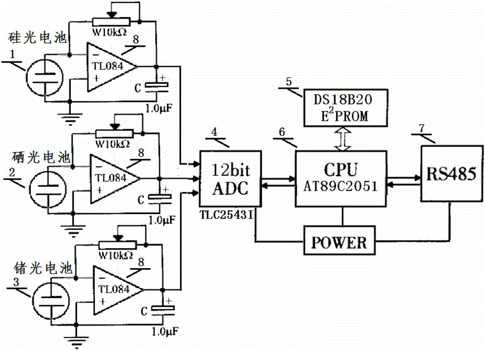
[0014] Including a variety of photocell sensors, AD chips, digital thermometers, MCU single-chip microcomputers, and RS485 bus chips. The photocell sensors are connected to the AD chips through a current-voltage conversion circuit. connect.
[0015] The various photocell sensors include selenium photocell sensors, silicon photocell sensors, and germanium photocell sensors.
[0016] The multiple photocell sensors transmit their short-circuit current electrical signals to the AD chip;
[0017] The MCU single-chip microcomputer controls the AD chip to collect current signals, and simultaneously reads the temperature value output by the digital thermometer and performs temperature compensation;
[0018] The MCU single-chip microcomputer obtains the insolation value according to the weighted summation of the output values of the various photocell sensors, and performs bus data t...
specific Embodiment
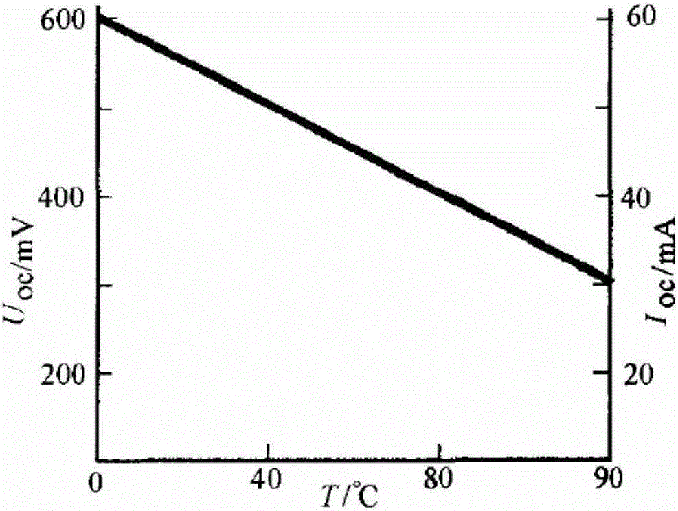
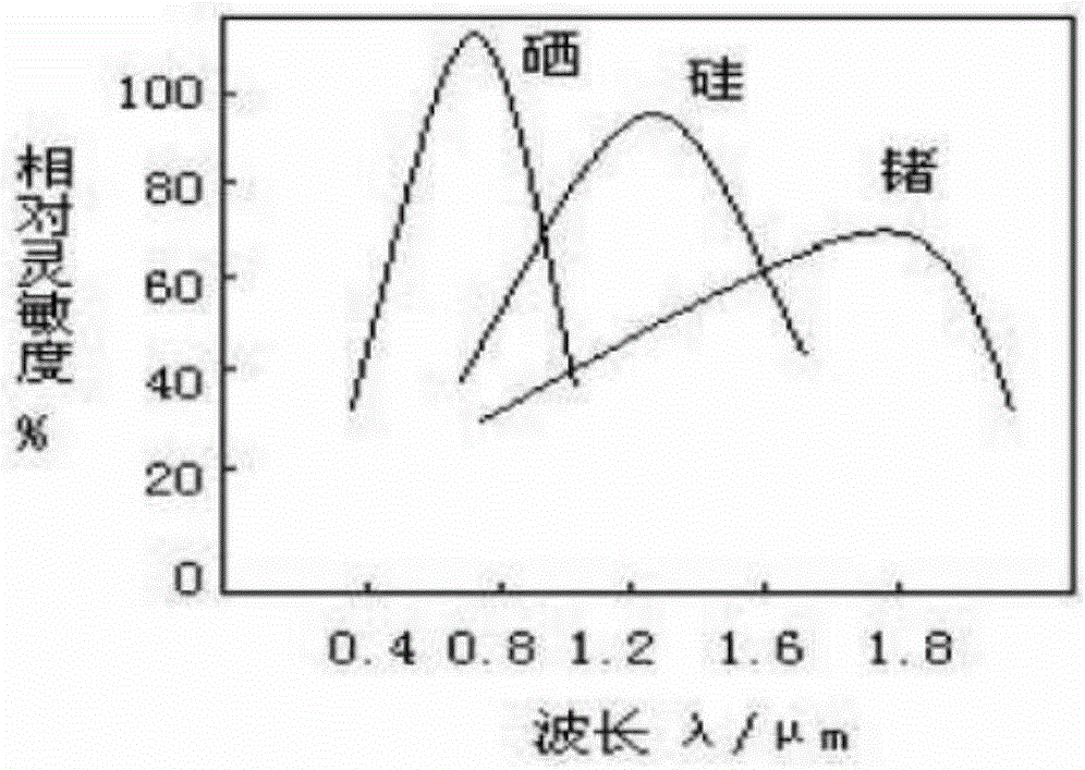
[0021] figure 1 It is the temperature characteristic curve of the silicon photovoltaic cell. figure 2 It is the spectral characteristic curve of silicon photovoltaic cell, germanium photovoltaic cell and selenium photovoltaic cell. Depend on figure 2 It can be seen that the incident wavelengths corresponding to the maximum sensitivity peaks of photocells of different materials are different. The spectral response peak of silicon photocells is around 0.8 μm, with a wavelength range of 0.4 to 1.2 μm, and the spectral response peak of selenium photocells is around 0.5 μm, with a wavelength range of 0.38 to 0.75 μm. .
[0022] Such as image 3 As shown, in order to try to overcome the defects of large temperature drift of photocells and the inability to feel the full spectrum of sunlight, a temperature sensor 6 is added to the measurement system to perform temperature compensation for the measurement, and multiple different types of silicon 1, selenium 2, and germanium 3 are ...
PUM
 Abstract
Description
Claims
Application Information
PatSnap Eureka turns technology decisions into work you can execute. Powered by our Innovation Knowledge Graph, it runs expert workflows across engineering, life sciences, materials and intellectual property. Get your review-ready output in minutes.


