Data reading method and system and data read/write method for PCIE (Peripheral Component Interconnect Express) SSD (Solid State Drive) array

A data reading and array technology, applied in the direction of electrical digital data processing, data processing input/output process, instruments, etc., can solve problems such as memory performance array performance bottlenecks, achieve the effect of reducing bandwidth pressure and improving performance

Active Publication Date: 2016-02-24
HUNAN GOKE MICROELECTRONICS
View PDF3 Cites 2 Cited by
  • Summary
  • Abstract
  • Description
  • Claims
  • Application Information

AI Technical Summary

Problems solved by technology

For example, the theoretical write bandwidth of an array composed of 48 Intel p3700 solid-state drives can reach 96GB / s, and the read bandwidth is even higher. In this case, the current memory performance has become the bottleneck of the array performance.

Method used


Image

  • Data reading method and system and data read/write method for PCIE (Peripheral Component Interconnect Express) SSD (Solid State Drive) array
  • Data reading method and system and data read/write method for PCIE (Peripheral Component Interconnect Express) SSD (Solid State Drive) array
  • Data reading method and system and data read/write method for PCIE (Peripheral Component Interconnect Express) SSD (Solid State Drive) array

Examples


Embodiment Construction

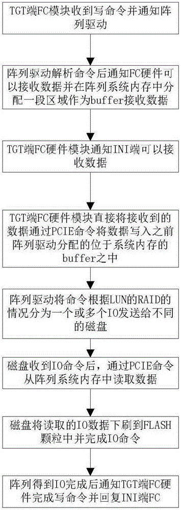
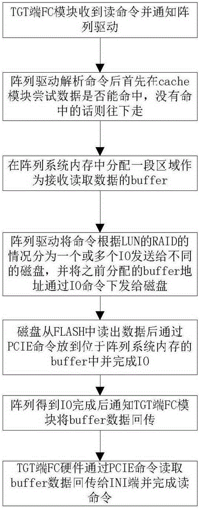
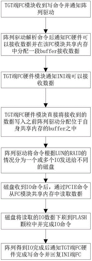
[0037] The present invention is based on a storage array using PCIESSD as a storage medium, and PCIESSD includes but not limited to SSD disks based on AHCI and NVMe protocols.

[0038] The present invention firstly requires the FC module at the TGT side to share a certain amount of its own memory with the array, which firstly requires the FC module to have its own memory controller and may require an external DDR. from image 3 and Figure 4 It can be seen that the biggest difference between the present invention and the existing solution is that the buffer and cache of IOdata are no longer located in the array system memory, but are located in the shared memory of the FC module. This solution has little impact on the current array architecture, and can also retain the cache hit and write-back characteristics of the read and write processes of the array itself. In addition, the array usually has multiple FC modules and multiple FCs sharing externally to provide LUN sharing s...


PUM


Abstract

The present invention discloses a data reading method and system and a data read/write method for a PCIE (Peripheral Component Interconnect Express) SSD (Solid State Drive) array. Buffer and cache of IO data is not located in an array system memory, but located in a shared memory of an FC module. According to the data reading method and system and the data read/write method for the PCIE SSD provided by the present invention, it is avoided that system memory performance becomes a bottleneck that constraints array performance; and additionally, because each PCIE SSD disk has a self memory, memory performance on the disk can be ensured not to be the bottle that constraints array and disk performances with the only need for ensuring that memory read/write performance in each disk can reach twice of a read/write bandwidth of the disk.

Description

technical field [0001] The invention relates to a data reading method, system and reading and writing method of a PCIESSD array. Background technique [0002] The existing operating systems and disk arrays are designed according to the fact that the performance of mechanical disks is far lower than that of memory. Compared with the read and write delays of mechanical disks, the read and write delays of memory are almost negligible, so whether it is The commonly used operating system is still the software architecture of the array. The data read and written are first stored in the system memory, and then sent to the disk or returned to the application. When reading, it will first check whether the data is hit in the memory cache. If it can be hit, it will be taken out of the memory cache and returned to the application. If it cannot be hit, it will be taken out from the disk and sent to the memory for the application. Let's take a look at the read and write process of the cu...

Claims


Application Information

Patent Timeline
Patent Type & Authority Applications(China)
IPC IPC(8): G06F3/06
CPCG06F3/0608G06F3/061G06F3/0689
Inventor 王翔向平周士兵姜黎马翼田达海彭鹏
Owner HUNAN GOKE MICROELECTRONICS
Why Eureka
Try Eureka