
Double-face welding method preventing big chip from falling off

A double-sided welding, large chip technology, applied in the direction of electrical components, printed circuit manufacturing, printed circuit, etc., can solve problems such as poor welding, lower production efficiency and output ratio, difficult maintenance, etc., to achieve good welding effect and reliable welding Effect

Active Publication Date: 2016-02-24
NANJING LUOPU TECH CO LTD
View PDF3 Cites 3 Cited by
  • Summary
  • Abstract
  • Description
  • Claims
  • Application Information

AI Technical Summary

Problems solved by technology

The display module needs to be welded on the front and back sides. Usually, the driving surface is welded first, and then the light-emitting tube part is welded. The reason is that the light-emitting tube cannot be reflowed twice. It is impossible to mount other chips on the display light-emitting surface except for the light-emitting tube.
Therefore, when the driving surface is mounted and the luminous tube is mounted upside down, the BGA package chip with a large self-weight will fall due to the influence of gravity, resulting in poor soldering
Due to the particularity of BGA packaging, product maintenance is more difficult, so if this problem is not solved, the production efficiency and output ratio will be greatly reduced
Of course, we can choose to solder the BGA-packaged chips on other printed boards and connect them through pins, but this method will increase the variety of products, reduce the reliability of the products, and increase the risk of the products

Method used


Image

  • Double-face welding method preventing big chip from falling off
  • Double-face welding method preventing big chip from falling off
  • Double-face welding method preventing big chip from falling off

Examples


Embodiment Construction

[0020] The present invention will be further described below in conjunction with embodiment.

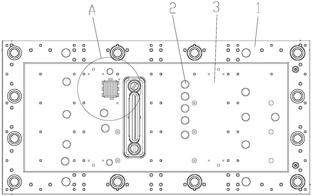
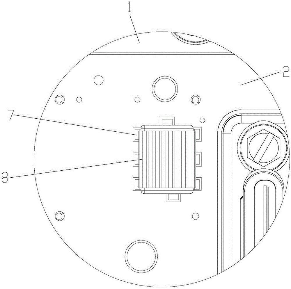
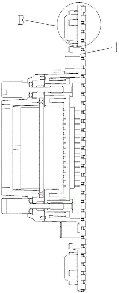
[0021] as attached Figure 1-5 The shown double-sided welding method for preventing large chips from coming off of the present invention comprises the following steps:

[0022] (1) Surface pretreatment: copper plating is carried out on the surface of the printed circuit board 1;

[0023] (2) Welding of the driving surface: lead-free soldering is selected, and various components 2 are welded on the driving surface 3 of the printed circuit board 1;

[0024] (3) BGA chip reinforcement: After welding the driving surface 3, dot red glue on the side of the BGA chip 4 for reinforcement;

[0025] (4) Welding of the light-emitting surface: lead welding is selected, and the light-emitting tube 5 is welded on the light-emitting surface 6 of the printed circuit board 1;

[0026] (5) Welding metal shielding case: increase metal shielding case 7 outside BGA chip 4, and metal shielding case 7 is...


PUM


Abstract

The invention discloses a double-face welding method preventing a big chip from falling off, belonging to the electronic member welding technology field. The double-face welding method comprises steps of (1) performing surface pre-processing, (2) welding a driving surface, (3) reinforcing a BGA chip, (4) welding a luminescence face, (5) welding a metal shielding housing, and (6) adhering a heat radiation sheet. The double-face welding method disclosed by the invention realizes reliable welding of double faces through welding temperature difference and can effectively prevent the BGA chip from falling off through reinforcing the BGA chip. The invention is good in the effect, and cannot cause BGA chip to fall off even that the shielding housing, the heat radiation sheets are added on the outside of the BGA chip.

Description

technical field [0001] The invention relates to a welding method for electronic components on a printed circuit board, in particular to a double-sided welding method for preventing large chips from falling off, and belongs to the technical field of electronic component welding. Background technique [0002] Display technology is changing with each passing day, picture quality is gradually improving, and display products are gradually becoming integrated and standardized. On the one hand, the receiving and storage part of the control card is designed in the display driver part; on the other hand, the voltage is increased and the current is reduced to meet the needs of various safety certifications. Therefore, the driving surface of the display module needs to add BGA-packaged chips. The display module needs to be welded on the front and back sides. Usually, the driving surface is welded first, and then the light-emitting tube part is welded. The reason is that the light-emit...

Claims


Application Information

Patent Timeline
Patent Type & Authority Applications(China)
IPC IPC(8): H05K3/34
CPCH05K3/3415H05K2203/047
Inventor 李农朱斌翁浙巍沈飞姜玲玲
Owner NANJING LUOPU TECH CO LTD
Learn More