Laser shock peening absorbing layer and clamping device thereof
A laser shock strengthening and absorption layer technology, applied in the field of laser processing, can solve problems such as affecting subsequent processing, affecting impact effect, and peeling off paint and workpiece surface.
- Summary
- Abstract
- Description
- Claims
- Application Information
AI Technical Summary
Problems solved by technology
Method used
Image
Examples
Embodiment 1
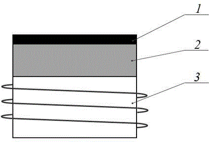
[0017] The absorbing layer 1 with a thickness of about 80 microns is coated on the surface of the workpiece 2 to be treated. The composition volume percentage of the absorbing layer 1 is: 6% ferric oxide particles with a particle size of 8-10 microns, 17% ferric oxide particles Carbon powder with a diameter of 8-10 microns, 70% binder and 5% additives. Among them, the components of the binder are: 70% water, 15% silicone oil, and 15% silicone resin, and the main components of the additives are stabilizers and defoamers.
[0018] After the absorbent layer 1 is dried in the air, perform the following steps: figure 1 As shown, the electromagnet 3 is installed on the back of the workpiece 2, and the electromagnet 3 is energized, and then the workpiece 1 is subjected to point-by-point laser shock peening. During the laser shock peening process, due to the impedance mismatch between the absorbing layer 1 and the surface of the workpiece 2, the A strong tensile stress is generated ...
Embodiment 2
[0021] The absorbing layer 1 with a thickness of about 100 microns is coated on the surface of the workpiece 2 to be treated. The volume percentage of the absorbing layer 1 is: 8% ferric oxide particles with a particle size of 8-10 microns, 12% ferric oxide particles Carbon powder with a diameter of 8-10 microns, 75% binder and 5% additives. Among them, the components of the binder are: 70% water, 15% silicone oil, and 15% silicone resin, and the main components of the additives are stabilizers and defoamers.
[0022] After the absorbent layer 1 is dried in the air, perform the following steps: figure 1 As shown, the electromagnet 3 is installed on the back of the workpiece 2, and the electromagnet 3 is energized, and then the workpiece 1 is subjected to point-by-point laser shock peening. During the laser shock peening process, due to the impedance mismatch between the absorbing layer 1 and the surface of the workpiece 2, the A strong tensile stress is generated at the inte...
PUM
| Property | Measurement | Unit |
|---|---|---|
| thickness | aaaaa | aaaaa |
| thickness | aaaaa | aaaaa |
| particle diameter | aaaaa | aaaaa |
Abstract
Description
Claims
Application Information
