Die pressing method of film circuit board

A circuit board and molding technology, which is applied in the field of film circuit board molding, can solve the problems of affecting film printing efficiency, cumbersome handling of plastic films, and difficulty in meeting process requirements, etc., and achieves small film deformation, high production efficiency, and good flatness Effect

Active Publication Date: 2016-03-02
FOSHAN NAN HAI DISTRICT SANJIAN PACKING CO LTD
View PDF6 Cites 1 Cited by
  • Summary
  • Abstract
  • Description
  • Claims
  • Application Information

AI Technical Summary

Problems solved by technology

However, the handling of plastic films is cumbersome, which often affects the printing efficiency of the film. Moreover, printing holographic patterns on the forward and reverse embossing surfaces of the plastic film has a negative effect on the printing on the forward and reverse embossing surfaces of the plastic film. The positioning accuracy of the graphics is very high, and the position error of the holographic images embossed on the front and back of the coating film must be less than 0.01mm. It is difficult to meet the process requirements by using two UV molding machines alone for molding.

Method used


Image

  • Die pressing method of film circuit board
  • Die pressing method of film circuit board
  • Die pressing method of film circuit board

Examples


Embodiment 1

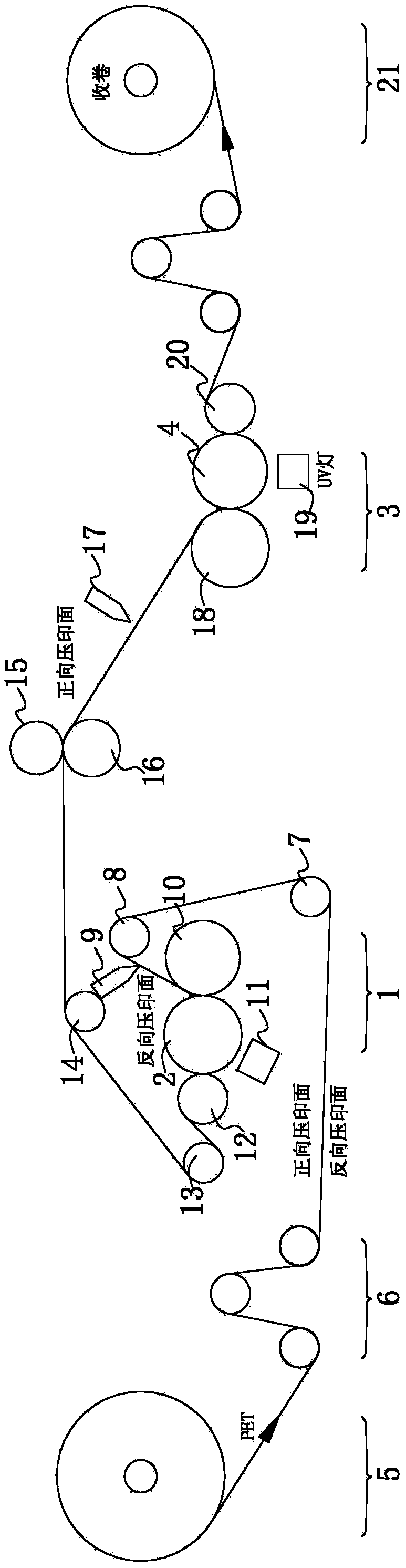
[0032] Taking the molded double-sided coated PET film as an example, in this embodiment 1, the positive embossing surface and the reverse embossing surface of the PET film are coated with a printing layer, and the printing layer is used to increase the UV coating and the PET film. The adhesion between the printing layer itself has no imaging function. The specific process of molding is as follows:

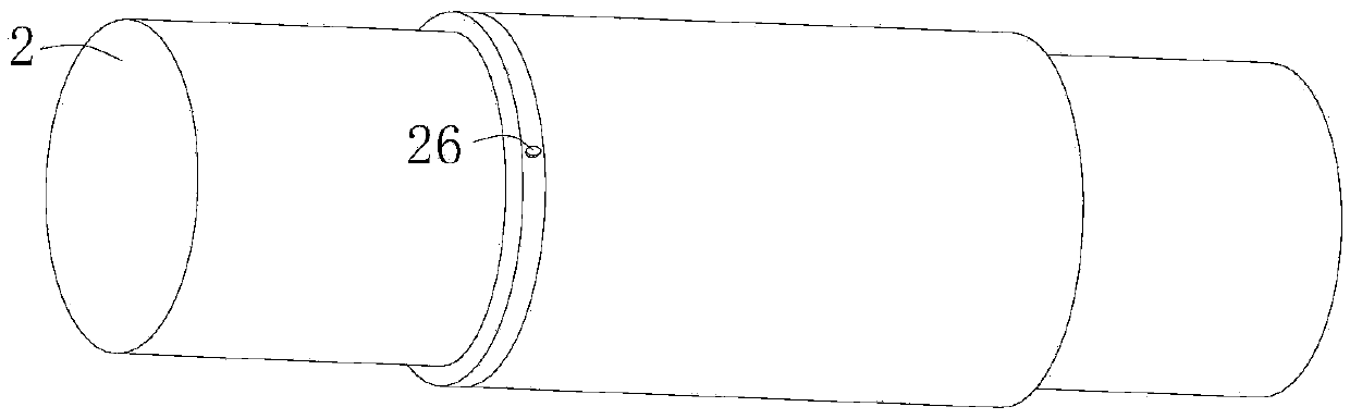
[0033] A) Use 3M strong double-sided adhesive tape to roll and paste a holographic metal nickel plate on the first plate roller 2 of the front UV molding system 1; the metal optical nickel plate is engraved with optical microstructures;

[0034] B) Use 3M strong double-sided adhesive tape to roll and stick a metal optical nickel plate on the second version roller 4 of the post-UV molding system 3, and the metal optical nickel plate is also engraved with optical microstructures;

[0035] C) according to the optical microstructure size on the metal optical nickel plate, such as the ...

Embodiment 2

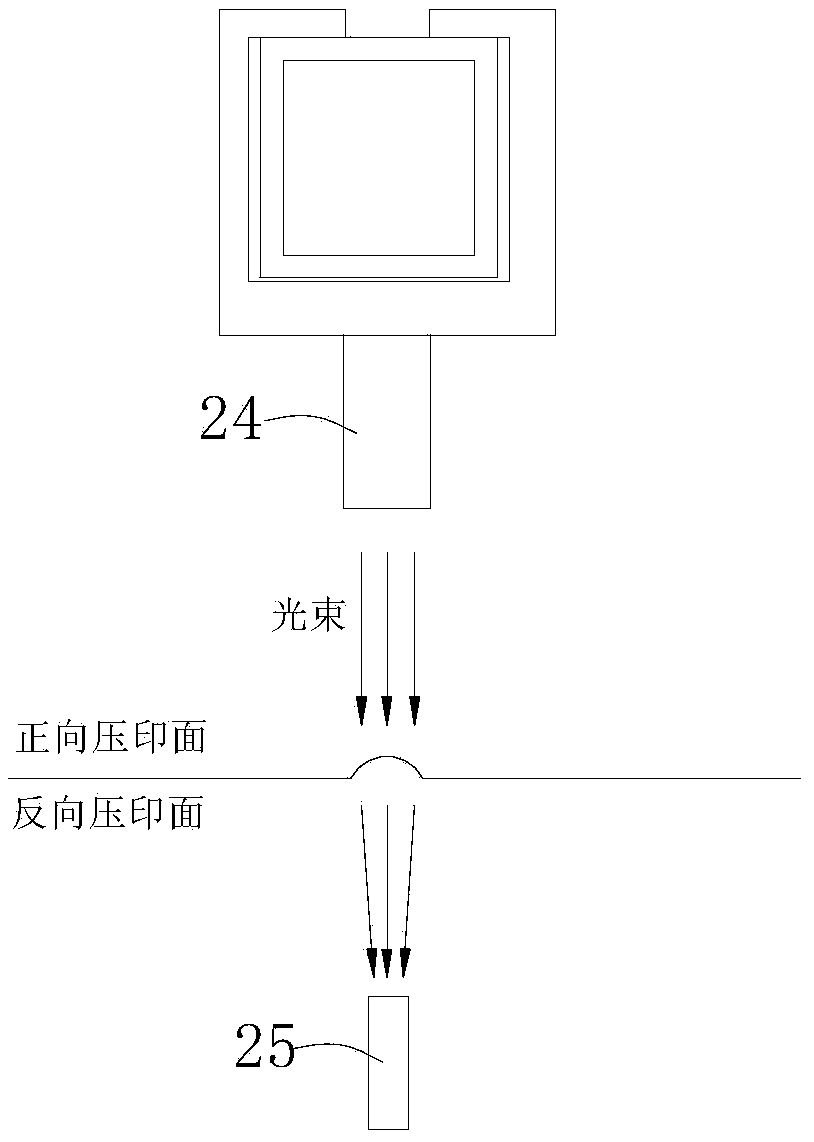
[0046] The difference between this embodiment 2 and embodiment 1 is that in this embodiment 2, the molding press used for molding the film also includes an adjustment system, which includes a positioning adjustment roller 22, a hydraulic cylinder 23, a detection light source 24 and A detection light source receiving device corresponding to the detection light source 24 ; the hydraulic cylinder 23 is used as a driving device, and its piston rod is connected with the positioning adjustment roller 22 . The detection light source receiving device includes a receiving probe 25 and a computer system, and the receiving probe 25 is data connected with the computer system; the hydraulic cylinder 23 is also data connected with the computer system through electronic components.

[0047] In the present embodiment 2, the molding process is as follows:

[0048] A) Utilize 3M strong double-sided adhesive tape to roll and stick metal optical nickel plate on the first version of roller 2, and ...


PUM

PropertyMeasurementUnit
reflectanceaaaaaaaaaa

Abstract

The invention discloses a die pressing method of a film circuit board. According to the die pressing method, a front reverse system and a rear reverse system are utilized, so that a front UV die pressing system and a rear UV die pressing system in front-and-rear connection can perform die pressing on the front stamping surface and the back stamping surface of a film; a regulating system is utilized, so that precise alignment of patterns on the front stamping surface and the back stamping surface which are die-pressed on the film are guaranteed. The die pressing method disclosed by the invention is precise to position, and the film does not need to be carried in the course of die pressing, so that the production efficiency is high. The deformation of the film in the production course is small, the planeness is good, and the produced film can meet the requirement of high quality.

Description

technical field [0001] The invention relates to a method for making a circuit board, in particular to a molding method for a thin film circuit board. Background technique [0002] Thin film circuit board is a flexible circuit board supported by PET film and has flexibility. At present, thin film circuit boards are widely used in electronic mechanical automation control, instrumentation, medical equipment, consumer electronics, computers, communications, metering, household appliances, toys, etc. [0003] At present, most of the production methods of film circuit boards on the market are to use two separate UV molding machines to respectively mold the positive embossing surface and the reverse embossing surface of the film. With this molding method, the operator needs to transfer the plastic film between two UV molding machines during the molding process. However, the handling of plastic films is cumbersome, which often affects the printing efficiency of the film. Moreover,...

Claims


Application Information

Patent Timeline
Patent Type & Authority Applications(China)
IPC IPC(8): B29C59/04
CPCB29C59/002B29C59/046
Inventor 吴小华
Owner FOSHAN NAN HAI DISTRICT SANJIAN PACKING CO LTD
Why Eureka
Try Eureka