Formation method of semiconductor structure

A semiconductor and gas technology, applied in semiconductor/solid-state device manufacturing, electrical components, circuits, etc., can solve the problems of semiconductor structure electrical performance and reliability to be improved, so as to improve reliability and electrical performance, improve appearance, prevent The effect of etching

Active Publication Date: 2016-03-02
SEMICON MFG INT (SHANGHAI) CORP
View PDF7 Cites 0 Cited by
  • Summary
  • Abstract
  • Description
  • Claims
  • Application Information

AI Technical Summary

Problems solved by technology

[0006] However, the electrical performance and reliability of existing

Method used


Image

  • Formation method of semiconductor structure
  • Formation method of semiconductor structure
  • Formation method of semiconductor structure

Examples


Embodiment Construction

[0038]It can be seen from the background art that the electrical performance and reliability of the semiconductor structure formed by using the TSV technology in the prior art needs to be improved.

[0039] It has been found through research that the performance of the redistribution layer (RDL, Redistribution Layer) located at the bottom and sidewall surface of the TSV via hole is poor. It is not covered by the rewiring layer, which is an important reason for the poor electrical performance and reliability of the semiconductor structure.

[0040] Conduct research on the formation method of the semiconductor structure, the process steps of forming the semiconductor structure include:

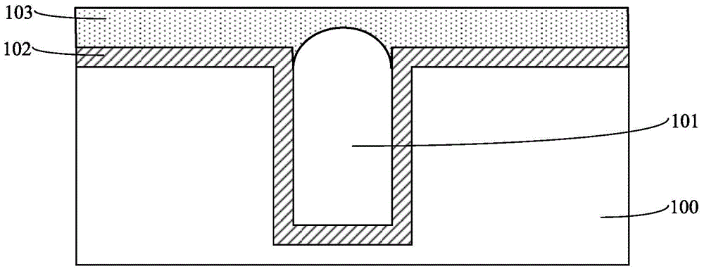
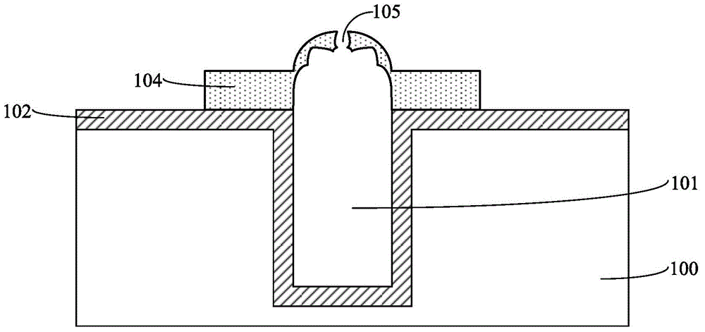
[0041] Please refer to figure 1 , providing a substrate 100, forming a through hole 101 in the substrate 100; forming a metal layer 102 on the surface of the substrate 100, the bottom and the sidewall surface of the through hole 101; using a spin-on-coating process (spin-on-coating) to form an...


PUM


Abstract

A formation method of a semiconductor structure comprises the following steps of providing a substrate, wherein a through hole is formed in the substrate; forming metal layers on a substrate surface, a through hole bottom and a sidewall surface; providing a lithography processing chamber, wherein pressure in the lithography processing chamber and pressure outside the lithography processing chamber possess a pressure difference, a pressure difference lithography technology is adopted in the lithography processing chamber, a photoresist layer is formed on a part of the metal layer surfaces, the photoresist layer closes the through hole and a gas is arranged in the through hole; taking the photoresist layer as a mask film, etching the metal layers till that a substrate surface is exposed and taking the residual metal layers as a redistribution layer; and removing the photoresist layer. By using the method of the invention, quality of the formed photoresist layer is increased; a thickness of the photoresist layer is avoided to be too thin or fracture is avoided; unnecessary etching to the metal layers of the through hole bottom and the sidewall surface is avoided too; quality of the formed redistribution layer is improved so that reliability and electric performance of the semiconductor structure are increased.

Description

technical field [0001] The invention relates to the technology in the field of semiconductor manufacturing, in particular to a method for forming a semiconductor structure. Background technique [0002] With the rapid development of semiconductor manufacturing technology, in order to achieve faster computing speed, larger data storage capacity and more functions of semiconductor devices, semiconductor chips are developing towards higher integration. The higher the integration degree of the semiconductor chip, the smaller the characteristic size (CD: Critical Dimension) of the semiconductor device. [0003] A three-dimensional integrated circuit (IC: Integrated Circuit) is manufactured using advanced chip stacking technology, which is to stack chips with different functions into an integrated circuit with a three-dimensional structure. Compared with two-dimensional integrated circuits, the stacking technology of three-dimensional integrated circuits can not only shorten the ...

Claims


Application Information

Patent Timeline
IPC IPC(8): H01L21/768H01L21/027
Inventor 何作鹏丁敬秀
Owner SEMICON MFG INT (SHANGHAI) CORP
Why Eureka
Try Eureka