

A kind of preparation method of tunneling field effect transistor
A tunneling field effect and transistor technology, applied in the direction of diodes, semiconductor devices, electrical components, etc., can solve the problems of unfavorable TFET device applications, difficult to realize TFET devices, slow concentration gradient at the source-drain junction, etc., to reduce production costs, Enhanced gate control ability, the effect of steep subthreshold slope
- Summary
- Abstract
- Description
- Claims
- Application Information
AI Technical Summary
Problems solved by technology
Method used
Image

Examples
Embodiment Construction
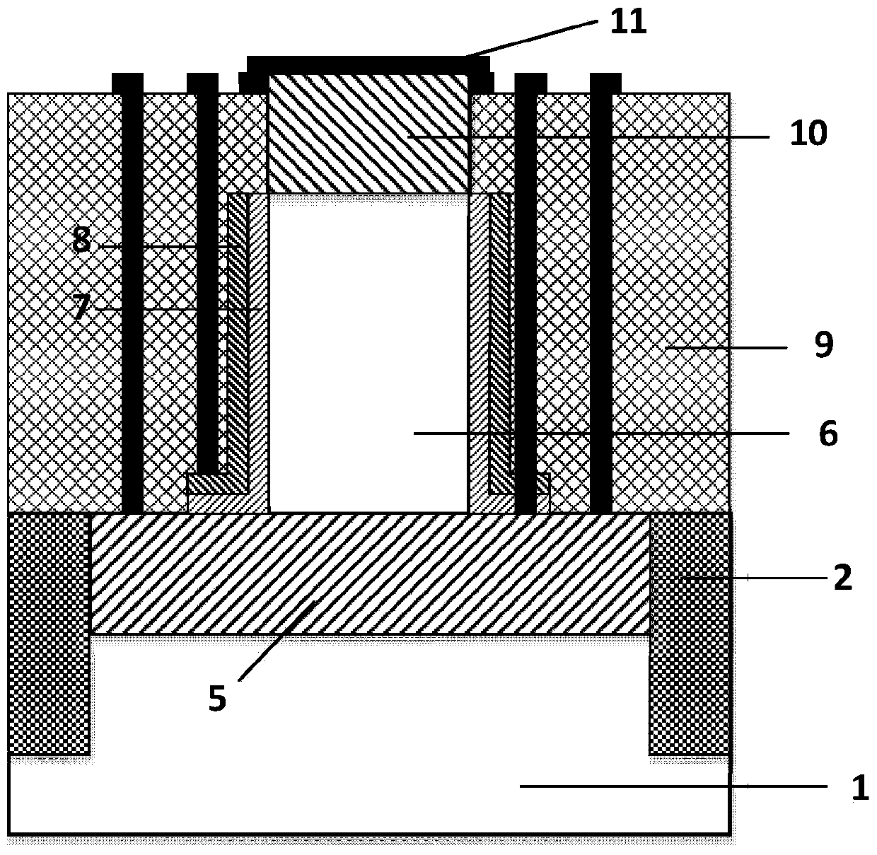
[0043] The implementation method of the tunneling field effect transistor for realizing the ultra-steep source junction of the present invention will be further described through specific embodiments below in conjunction with the accompanying drawings.
[0044] The specific implementation steps are as Figure 1-Figure 8 Shown: (This example takes N-type devices as an example, and P-type devices can be deduced by analogy)
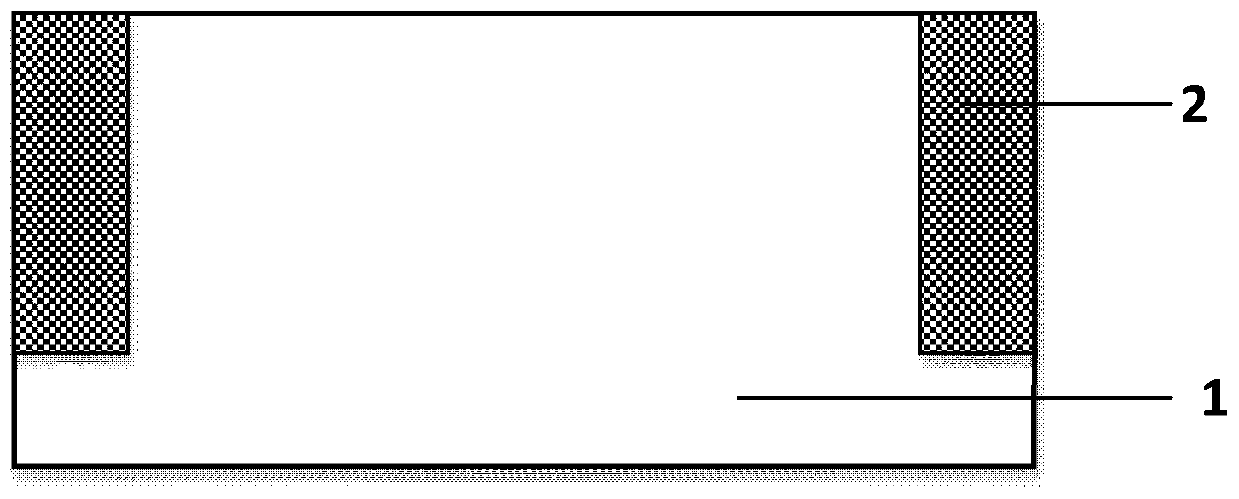
[0045] 1. The substrate doping concentration is lightly doped (about 1E13cm -3 -1E15cm -3 ), a layer of silicon dioxide is initially thermally oxidized on the Si substrate 1 with a crystal orientation of , with a thickness of about 10 nm, and a layer of silicon nitride (Si 3 N 4 ), with a thickness of about 100nm, and then use shallow trench isolation technology to make STI isolation 2 in the active area, and then perform CMP, such as figure 2 shown;
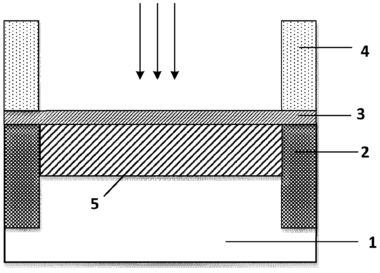
[0046] 2. Thermal oxidation to form the implantation barrier layer 3, photolithography exposes the tu...
PUM
 Abstract
Description
Claims
Application Information