Nano-sheet ring-gate field effect transistor with double-layer side wall structure

A field-effect transistor and sidewall structure technology, which is applied in the field of field-effect transistor logic devices, can solve problems such as serious self-heating effects, achieve the effects of alleviating self-heating effects, enhancing coupling effects, and reducing thermal resistance

Active Publication Date: 2019-09-17
EAST CHINA NORMAL UNIV +1
View PDF4 Cites 5 Cited by
  • Summary
  • Abstract
  • Description
  • Claims
  • Application Information

AI Technical Summary

Problems solved by technology

[0003] The present invention aims at the problem of serious self-heating effect of the existing nano-sheet ring gate field effect transistor using high dielectric constant materials such as hafnium dioxide, and alleviates the self-heating effect of the device on the basis that the device still has a large on-state current , proposed a nanosheet gate-all-around field-effect transistor with a double-layer sidewall structure

Method used


Image

  • Nano-sheet ring-gate field effect transistor with double-layer side wall structure
  • Nano-sheet ring-gate field effect transistor with double-layer side wall structure
  • Nano-sheet ring-gate field effect transistor with double-layer side wall structure

Examples


Embodiment

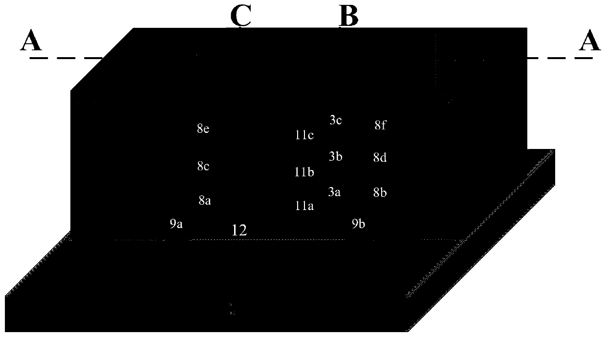
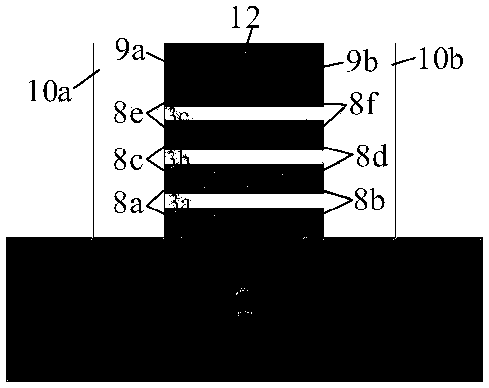
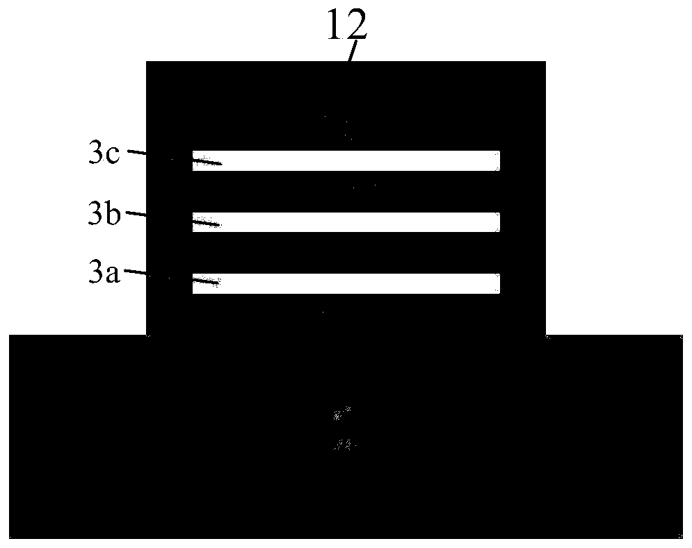
[0031] In this embodiment, the channel region is vertically stacked with three layers as an example.

[0032] refer to Figure 1 to Figure 4 The nanosheet gate-all-around field effect transistor with a double-layer sidewall structure proposed by the present invention includes the following structures: nanosheet channel regions 3a, 3b, 3c, gate dielectric layers 11a, 11b, 11c, gate metal layer 12, Substrate 1, raised source 10a, raised drain 10b, source low-k sidewalls 8a, 8c, 8e, source high-k sidewalls 9a, drain low-k sidewalls 8b, 8d, 8f and drain end high-k sidewall 9b, the nanosheet channel regions 3a, 3b, 3c are composed of three vertically stacked channels, and the periphery of each vertically stacked channel is sequentially provided with source end low-k sidewalls 8a along the horizontal direction . The low-k sidewalls 8a, 8c, and 8e at the source end have three layers, and each layer does not touch; the low-k sidewalls 8b, 8d, and 8f at the drain end have three layer...


PUM


Abstract

The invention discloses a nano-sheet ring-gate field effect transistor with a double-layer side wall structure. The device has two layers of side walls, a side wall close to a nano-sheet channel is made of a material with a low dielectric constant (low-k for short) and high thermal conductivity, and a side wall away from the nano-sheet channel is made of a material with a high dielectric constant (high-k for short). The side wall formed by the low-k material facilitates the heat radiation of the device, the side wall formed by the high-k material facilitates the reinforcement of the coupling between a device gate and the channel, and therefore, the device still has good heat dissipation effect under a large on-state current condition. In addition, the heat dissipation capability and DC performance of the device can be flexibly regulated by changing the thickness ratio of the low-k material to the high-k material.

Description

technical field [0001] The invention belongs to the field effect transistor logic device technical field of CMOS very large-scale integrated circuit (VLSI), in particular to a nanosheet ring gate field effect transistor with a double-layer side wall structure and a preparation method thereof. Background technique [0002] When the semiconductor process node develops to the nanometer level, in order to meet the requirements of reducing the feature size of the transistor, the aspect ratio of the fin field-effect transistor (Fin Field-Effect Transistor, referred to as FinFET) continues to increase, which is very important for FinFET devices. Both the manufacturing process and the ability to suppress short-channel effects have brought great challenges. In order to promote the development of semiconductor devices to smaller process nodes, the Stacked Nanosheet Gate-All-Around Field-Effect Transistor (NS-GAAFET for short), with its excellent gate control ability and flexible The ...

Claims


Application Information

Patent Timeline
Patent Type & Authority Applications(China)
IPC IPC(8): H01L29/78H01L29/08H01L21/336
CPCH01L29/0847H01L29/66795H01L29/785
Inventor 刘人华王昌锋田明黄琴李小进孙亚宾石艳玲廖端泉曹永峰
Owner EAST CHINA NORMAL UNIV
Why Eureka
Try Eureka